Laser Debonding Equipment Market Size, Share & Industry Analysis, By Technology (Laser Ablation, Laser-Induced Forward Transfer), By Laser Type (UV Laser, IR Laser) and Regional Forecast, 2026-2034
 Download Free Sample
Laser Debonding Equipment Market Overview
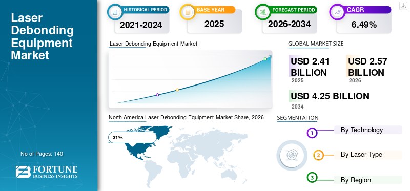
The laser debonding equipment market size was valued at USD 2.41 billion in 2025. The market is projected to grow from USD 2.57 billion in 2026 to USD 4.25 billion by 2034, exhibiting a CAGR of 6.49% during the forecast period.

The laser debonding equipment market is becoming a critical segment of the semiconductor manufacturing ecosystem due to the growing use of advanced packaging technologies, wafer thinning processes, and heterogeneous integration. Laser debonding equipment enables precise separation of temporary bonded wafers without causing mechanical stress or substrate damage. The increasing production of ultra-thin wafers, 3D integrated circuits, MEMS devices, image sensors, and power semiconductors has accelerated the adoption of laser debonding systems. The laser debonding equipment market report highlights strong demand from semiconductor fabrication plants, outsourced semiconductor assembly providers, and advanced electronics manufacturers seeking higher production yields and improved process reliability.
Download Free sample to learn more about this report.
USA Market Overview
The United States remains a significant contributor to the laser debonding equipment market due to its strong semiconductor research capabilities, advanced manufacturing infrastructure, and ongoing investments in domestic chip production. The presence of major semiconductor fabrication facilities and packaging technology developers supports continuous adoption of laser debonding solutions for wafer-level packaging and chiplet integration applications.
Demand in the U.S. market is increasingly linked to advanced computing, artificial intelligence processors, automotive electronics, aerospace systems, and defense-grade semiconductor components. The Laser Debonding Equipment industry analysis indicates that manufacturers are prioritizing non-contact debonding methods to enhance production efficiency while minimizing wafer breakage and contamination risks.
Laser Debonding Equipment Market Key Takeaways
 Global Market Size & Forecast
- 2025 Market Size: USD 2.41 Billion
- 2026 Market Size: USD 2.57 Billion
- 2034 Forecast Market Size: USD 4.25 Billion
- CAGR: 6.49% from 2026-2034
 Market Share
- The market in Asia-Pacific dominated with a revenue share of 38% in 2025.
- Laser Ablation dominated by technology with a market share of approximately 62%.
- UV Laser systems dominated by laser type with a market share of approximately 68%.
 Key Regional Highlights
Asia-Pacific
Asia-Pacific led the market with a 38% share, supported by expanding semiconductor manufacturing and advanced packaging activities.
North America
North America accounted for 31% of the market, driven by strong investments in semiconductor fabrication and advanced electronics.
Europe
Europe held a 24% share, supported by established semiconductor manufacturing and technology development.
U.S
The U.S. remains a key market, supported by advanced semiconductor manufacturing and investments in next-generation packaging technologies.
Japan
Japan accounted for approximately 22% of the Asia-Pacific market, supported by its established semiconductor and electronics manufacturing industry.
Read More

laser debonding equipment market Latest trends
One of the most significant laser debonding equipment market trends is the increasing deployment of ultraviolet laser systems for temporary wafer bonding and debonding applications. UV laser technologies provide enhanced precision, lower thermal impact, and superior compatibility with advanced semiconductor packaging processes. Manufacturers are integrating automated handling systems, artificial intelligence-assisted process monitoring, and real-time inspection capabilities into laser debonding platforms.
Download Free sample to learn more about this report.
Another notable trend involves the growing demand for ultra-thin semiconductor wafers below 50 microns. Advanced packaging technologies such as fan-out wafer-level packaging, 3D stacking, and chiplet architectures require sophisticated debonding equipment capable of preserving substrate integrity. The laser debonding equipment market research report also identifies rising adoption in flexible displays, OLED manufacturing, MEMS fabrication, and power semiconductor production. Automation, higher throughput rates, reduced particle contamination, and improved energy efficiency continue to shape equipment development strategies across the industry.
laser debonding equipment market Dynamics
DRIVER
Rising Demand for Advanced Semiconductor Packaging Technologies
The primary growth driver in the laser debonding equipment market is the increasing adoption of advanced semiconductor packaging solutions. Modern electronic devices require smaller form factors, higher computing power, and improved energy efficiency. To meet these requirements, manufacturers are utilizing wafer thinning, 3D integration, heterogeneous integration, and chiplet-based architectures that depend heavily on temporary wafer bonding and laser debonding processes.
Laser debonding equipment provides precise and non-contact wafer separation, reducing substrate damage while improving production yields. Semiconductor manufacturers increasingly rely on laser-based systems to process ultra-thin wafers used in artificial intelligence accelerators, memory devices, image sensors, automotive chips, and advanced communication components. As advanced packaging becomes a core manufacturing strategy, demand for laser debonding equipment continues to expand across fabrication facilities worldwide.
RESTRAINT
High Equipment Acquisition and Implementation Costs
A major restraint affecting the laser debonding equipment market is the substantial investment required for equipment procurement, installation, and maintenance. Advanced laser debonding systems incorporate precision optics, automation modules, wafer handling mechanisms, and process monitoring technologies that contribute to high capital expenditures.
Small and medium-sized semiconductor manufacturers often face budget limitations when considering adoption of laser debonding solutions. In addition, integration into existing production lines requires process optimization, workforce training, and compatibility assessments with temporary bonding materials. Maintenance requirements for laser sources and optical components can further increase operational expenses. These factors may slow deployment among cost-sensitive manufacturing facilities despite the long-term productivity benefits associated with laser debonding technologies.
OPPORTUNITY
Expansion of Flexible Electronics and Advanced Display Manufacturing
The rapid development of flexible electronics represents a major opportunity for the laser debonding equipment market. Flexible displays, foldable smartphones, wearable devices, medical sensors, and advanced OLED technologies increasingly require temporary carrier substrates during manufacturing. Laser debonding provides a reliable solution for separating delicate flexible structures without causing deformation or performance degradation.
Manufacturers are also exploring laser debonding technologies for next-generation display panels, micro-LED production, and large-area electronics. As consumer demand for lightweight and flexible devices increases, equipment suppliers have opportunities to introduce specialized debonding platforms optimized for non-semiconductor applications. This diversification broadens the addressable market and creates additional revenue streams for equipment developers and process technology providers.
CHALLENGE
Maintaining Process Uniformity for Ultra-Thin Wafers
One of the most significant challenges in the laser debonding equipment market is achieving consistent process uniformity across increasingly thin and fragile wafers. As semiconductor manufacturers reduce wafer thickness to support advanced packaging architectures, the risk of warpage, cracking, and thermal stress becomes more pronounced.
Laser energy distribution must remain highly uniform across large wafer surfaces to prevent localized damage and yield losses. Variations in adhesive materials, substrate compositions, and wafer dimensions further complicate process optimization. Equipment manufacturers must continually develop improved beam shaping technologies, precision alignment systems, and advanced process control software to meet evolving industry requirements. Failure to maintain process consistency can negatively affect production efficiency and device performance.
laser debonding equipment market Segmentation
By Technology
Laser Ablation technology dominates the laser debonding equipment market with an estimated market share of 62%. This technology utilizes focused laser energy to selectively remove adhesive layers or weaken bonding interfaces between temporary carriers and semiconductor wafers. Its popularity stems from high precision, reduced mechanical stress, and compatibility with advanced semiconductor manufacturing processes.
The technology is widely used in wafer thinning operations, advanced packaging facilities, and high-volume semiconductor production environments. Laser Ablation systems support improved throughput, reduced contamination, and excellent substrate protection. The laser debonding equipment market analysis indicates continued demand from manufacturers producing advanced processors, memory chips, MEMS devices, and image sensors. Increasing investments in semiconductor fabrication facilities further strengthen the position of Laser Ablation technology within the global market.
Laser-Induced Forward Transfer accounts for approximately 38% of the laser debonding equipment market. This technology offers precise material transfer and selective energy delivery capabilities, making it suitable for specialized semiconductor packaging applications and emerging electronics manufacturing processes.
Laser-Induced Forward Transfer is increasingly utilized where minimal thermal impact and exceptional process control are required. Applications include flexible electronics manufacturing, advanced sensor production, and high-value semiconductor devices. The technology supports innovative packaging designs and enables manufacturers to process delicate substrates that may be unsuitable for traditional debonding approaches. Ongoing research and development activities continue to improve system performance and expand commercial adoption across advanced manufacturing sectors.
To know how our report can help streamline your business, Speak to Analyst
By Laser Type
UV Laser systems represent approximately 68% of the laser debonding equipment market. These systems are preferred due to their ability to selectively interact with temporary bonding materials while minimizing damage to semiconductor substrates. UV lasers provide excellent precision and are widely used for wafer-level packaging, 3D integration, and ultra-thin wafer processing.
The growing adoption of advanced semiconductor packaging technologies has accelerated demand for UV laser debonding equipment. Manufacturers value the technology for its high process reliability, reduced contamination levels, and compatibility with next-generation packaging architectures. UV laser systems are particularly important in the production of high-performance computing chips, advanced memory devices, and artificial intelligence processors.
IR Laser systems hold an estimated 32% share of the laser debonding equipment market. These systems are used in applications requiring deeper energy penetration and compatibility with specific substrate materials and adhesive formulations.
IR laser debonding equipment is gaining traction in specialized manufacturing environments, including power semiconductor production and certain display fabrication processes. Equipment developers continue to improve beam quality, energy efficiency, and process control capabilities to enhance competitiveness. While UV systems dominate mainstream semiconductor applications, IR lasers maintain an important role in niche manufacturing segments where unique material characteristics influence technology selection.
laser debonding equipment market Regional outlook
North America Laser Debonding Equipment Market Share, 2026 (%)
To get more information on the regional analysis of this market, Download Free sample
North America
North America accounts for approximately 31% of the laser debonding equipment market. The region benefits from advanced semiconductor manufacturing infrastructure, substantial research investments, and strong demand for high-performance electronic components. Semiconductor packaging facilities increasingly utilize laser debonding systems to support wafer thinning and heterogeneous integration processes.
Growing investments in domestic semiconductor production and advanced packaging capabilities continue to strengthen regional demand. Automotive electronics, aerospace applications, defense systems, and AI-related semiconductor products contribute significantly to equipment adoption.
Europe
Europe represents approximately 24% of the laser debonding equipment market. The region is characterized by strong engineering expertise, advanced manufacturing capabilities, and extensive research activities focused on semiconductor process innovation.
European manufacturers are increasingly investing in advanced packaging technologies to strengthen supply chain resilience and improve semiconductor production capacity. Laser debonding equipment adoption is supported by demand from automotive electronics, industrial automation, and advanced sensor manufacturing sectors.
Germany laser debonding equipment market
Germany accounts for approximately 34% of the European laser debonding equipment market. The country's leadership in semiconductor equipment engineering, precision manufacturing, and industrial automation supports strong demand for advanced debonding systems.
German semiconductor companies and research institutions continue to invest in wafer-level packaging, MEMS fabrication, and power electronics manufacturing. The market benefits from strong collaboration between equipment suppliers, technology developers, and industrial end users. Advanced automotive semiconductor production remains a major contributor to laser debonding equipment demand.
United Kingdom laser debonding equipment market
The United Kingdom holds approximately 18% of the European laser debonding equipment market. The market is supported by research-intensive semiconductor activities, photonics development programs, and specialized electronics manufacturing operations.
Investment in semiconductor innovation, advanced materials research, and next-generation packaging technologies contributes to increasing adoption of laser debonding systems. The UK also benefits from growing demand for semiconductor components used in telecommunications, defense, medical technology, and industrial automation applications.
Asia-Pacific
Asia-Pacific dominates the laser debonding equipment market with approximately 38% share. The region hosts a large concentration of semiconductor fabrication facilities, packaging plants, display manufacturers, and electronics production centers.
Rapid growth in advanced packaging technologies, memory device manufacturing, and consumer electronics production supports continuous demand for laser debonding equipment. Regional manufacturers prioritize high-throughput and automated solutions to meet increasing production requirements.
Japan laser debonding equipment market
Japan accounts for approximately 22% of the Asia-Pacific laser debonding equipment market. The country's expertise in semiconductor manufacturing equipment, precision laser systems, and advanced materials supports strong market development.
Japanese manufacturers continue to invest in image sensors, power semiconductors, MEMS devices, and advanced packaging technologies. The emphasis on manufacturing quality and process optimization contributes to widespread adoption of sophisticated laser debonding solutions.
China laser debonding equipment market
China represents approximately 41% of the Asia-Pacific laser debonding equipment market. Expanding semiconductor manufacturing capacity, government-backed industrial initiatives, and rising investments in advanced packaging facilities support strong market growth.
Domestic semiconductor producers increasingly deploy laser debonding systems to improve manufacturing efficiency and reduce reliance on imported technologies. The country's large-scale electronics production ecosystem further accelerates equipment adoption across multiple end-use industries.
Rest of World
The Rest of World region accounts for approximately 7% of the laser debonding equipment market. Emerging semiconductor manufacturing investments, growing electronics production, and increasing adoption of advanced packaging technologies support gradual market expansion.
Countries in the Middle East, Latin America, and selected African markets are exploring semiconductor development opportunities. Although adoption levels remain lower than in established regions, growing industrial modernization initiatives create long-term opportunities for equipment suppliers.
List of Top Laser Debonding Equipment Companies
- Shin-Etsu Engineering Co., LTD.
- EV Group (EVG)
- SUSS MicroTec SE
- CWI Technical
- Kingyoup Enterprises Co., Ltd
- Optec S.A.
- Brewer Science, Inc.
- Tokyo Electron Limited
- SuperbIN Co. Ltd.
- Han's Laser Technology industry Group Co., Ltd
Top Two Companies by Market share
- EV Group (EVG) – 24%
- SUSS MicroTec SE – 19%
Investment analysis and opportunities
Investment activity in the laser debonding equipment market continues to increase as semiconductor manufacturers expand advanced packaging capabilities. Capital expenditures are focused on wafer-level packaging facilities, heterogeneous integration technologies, and production lines supporting artificial intelligence processors, memory devices, and power semiconductors.
The strongest opportunities are emerging in Asia-Pacific manufacturing hubs, advanced packaging centers in North America, and semiconductor modernization projects across Europe. Investors are prioritizing companies developing automated debonding systems, advanced laser technologies, intelligent process monitoring software, and next-generation wafer handling solutions. Additional opportunities exist in flexible electronics manufacturing, OLED production, micro-LED applications, and advanced sensor fabrication. Equipment suppliers that can deliver higher throughput, lower operating costs, and improved yield performance are expected to benefit from long-term industry expansion.
New Product Development
Product development efforts within the laser debonding equipment market are increasingly focused on automation, precision control, and process optimization. Manufacturers are introducing systems featuring advanced beam shaping technologies, artificial intelligence-assisted monitoring, and integrated inspection modules capable of identifying process deviations in real time.
Recent innovations include high-speed wafer handling platforms, multi-wavelength laser configurations, advanced thermal management systems, and improved substrate alignment technologies. Equipment developers are also working on solutions specifically designed for ultra-thin wafers, chiplet integration architectures, and flexible electronic devices. Enhanced software capabilities, predictive maintenance functions, and smart factory compatibility are becoming key differentiators among next-generation laser debonding platforms.
Five Recent Developments (2023-2025)
- EV Group expanded advanced wafer debonding solutions for heterogeneous integration applications.
- SUSS MicroTec introduced enhanced temporary bonding and debonding platforms supporting advanced packaging processes.
- Han's Laser expanded fully automated laser debonding equipment offerings for semiconductor manufacturing.
- Shin-Etsu Engineering advanced UV laser debonding systems for ultra-thin semiconductor wafer processing.
- Multiple equipment manufacturers integrated AI-based process monitoring and automation capabilities into laser debonding platforms.
report Coverage
The laser debonding equipment market report provides comprehensive coverage of technology developments, market dynamics, segmentation analysis, regional outlook, competitive landscape, and investment opportunities. The report evaluates industry trends affecting semiconductor manufacturing, advanced packaging technologies, flexible electronics production, and wafer-level processing applications.
Request for Customization to gain extensive market insights.
The scope includes detailed assessment of laser ablation technologies, laser-induced forward transfer systems, UV laser platforms, and IR laser solutions. It further examines regional demand patterns, competitive positioning of leading manufacturers, emerging application areas, and technological innovations shaping future industry development. The laser debonding equipment market research report serves as a strategic resource for semiconductor manufacturers, equipment suppliers, investors, technology developers, and industry stakeholders seeking actionable market insights.
Frequently Asked Questions
Fortune Business Insights says that the global market value stood at USD 2.41 billion in 2025 and is projected to reach USD 4.25 billion by 2034.
The market is expected to exhibit a CAGR of 6.49% during the forecast period of 2026-2034.
Laser Ablation led the technology segment with an estimated 62% share, owing to its high precision, reduced mechanical stress, and compatibility with advanced semiconductor manufacturing.
Key players include Shin-Etsu Engineering Co., LTD.; EV Group (EVG); SUSS MicroTec SE; CWI Technical; Kingyoup Enterprises Co., Ltd.; and Optec S.A.
Major trends include increasing deployment of UV laser systems with automated and AI-assisted process monitoring and growing demand for equipment supporting ultra-thin wafers, 3D stacking, and chiplet architectures. Asia-Pacific led the market with a 38% share.
- 2021-2034
- 2025
- 2021-2024
- 140
-

(Offer valid till 30th Sep 2026)
Get 30-60 hrs Free Customization
Expand Regional and Country Coverage, Segments Analysis, Company Profiles, Competitive Benchmarking, and End-user Insights.













-
US +1 833 909 2966 ( Toll Free )
-
Get In Touch With Us