Nano Metrology Market Size, Share & Industry Analysis, By Type (Hardware and Software Solutions), By Sales Channel (Direct Channels and Indirect Channels), By End User (Material Science, Energy & Power, Industrial Manufacturing Companies, Electronics & Semiconductor Manufacturers, Healthcare & Life Sciences, and Aerospace & Defense Contractors), and Regional Forecast, 2026-2034
Nano Metrology Market Size and Future Outlook
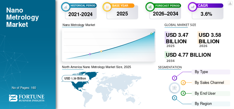
The global nano metrology market size was valued at USD 3.47 billion in 2025. The market is projected to grow from USD 3.58 billion in 2026 to USD 4.77 billion by 2034, exhibiting a CAGR of 3.6% during the forecast period. North America dominated the nano metrology market with a market share of 40.06% in 2025.
Nano metrology refers to instruments and devices that measure structures, materials, and devices at the nanoscale. Evolving energy systems, growing demand for non-engineered materials, precision engineering, and 3D architectures are all driving the growth of nanometrology. Nano-technology is gaining further traction in healthcare & life sciences through drug delivery, tissue engineering, diagnostics, and nanomedicine.
- For instance, in June 2024, Gleason introduced the 175GMS nano Gear Metrology system with minimal noise, enhanced precision, and extended gear life.
Key players such as Bruker Corporation, Keysight Technologies, Olympus Corporation, and KLA Corporation are heavily investing in research and technology. Rising R&D investments in nanotechnology, miniaturization trends, and the high demand for yield improvement are expected to drive market share.
Download Free sample to learn more about this report.
Nano Metrology Market Key Takeaways
- 2025 Market Size: USD 3.47 Billion
- 2026 Market Size: USD 3.58 Billion
- 2034 Forecast Market Size: USD 4.77 Billion
- CAGR: 3.6% from 2026–2034
- North America dominated the nano metrology market with a 40.06% share in 2025.
- The hardware segment held the largest market share due to widespread deployment of advanced measurement instruments.
- Direct sales channels dominated the market, driven by demand for customized systems and technical support.
North America
North America led the global market, generating more than USD 1.39 billion in revenue in 2025.
Asia Pacific
Asia Pacific is the fastest-growing region, supported by expanding semiconductor manufacturing and research investments.
Europe
Europe maintains a significant market presence due to strong industrial and scientific research activities.
U.S.
The market is expected to reach USD 1.09 billion in 2026, leading the North American region.
Japan
Strong semiconductor and precision manufacturing industries continue to support market growth.
Read More
NANO METROLOGY MARKET TRENDS
AI/ML-Enabled Nano Metrology to Gain Momentum Supporting Complex and Data-Intensive Systems
Industry 4.0 and smart manufacturing initiatives to drive the adoption of AI in nano metrology. Several tools, such as AFM, optical systems, and TEM, produce massive amounts of high-resolution data. Rapid processing of such multidimensional data requires AI that reduces manual errors and enables automated pattern recognition. AI/ML enables noise filtering and signal enhancement, resulting in increased precision and advanced manufacturing. AI/ML enables self-optimizing and autonomous measurement systems that operate directly on production lines.
- For example, in September 2025, Onto Innovation Inc. introduced the OCD metrology system Atlas G6.
Download Free sample to learn more about this report.
MARKET DYNAMICS
MARKET DRIVERS
Rapid Miniaturization & Advanced Manufacturing Requirements Driving Growth in the Nano Metrology Industry
The nano metrology market growth is primarily driven by the rapid miniaturization of components across industries such as semiconductors, electronics, and advanced manufacturing. As device geometries shrink to the nanometer scale, conventional measurement techniques become inadequate, creating a strong need for highly precise and reliable nano metrology solutions. Growing investments in advanced semiconductor nodes, 3D ICs, MEMS, and nanomaterials have further intensified the requirement for accurate dimensional, surface, and thin-film measurements.
The rising adoption of nanotechnology in energy storage, healthcare, and aerospace applications has increased the complexity of the materials and structures being measured. This, in turn, is pushing manufacturers to deploy advanced microscopes, nano positioning systems, and high-resolution measuring instruments. Consequently, demand for nanometrology solutions continues to grow as industries focus on improving yield, quality control, and process efficiency.
- For instance, in February 2024, Bruker Corporation acquired Nanophoton Corporation to expand its nanotechnology capabilities.
MARKET RESTRAINTS
High Capital Cost & Technical Complexity to Limit Market Adoption
The market is constrained by the high capital costs and technical complexity associated with advanced measurement equipment, such as AFM, SEM, and CD-SEM systems. These tools require significant upfront investment, specialized infrastructure, and skilled operators, which can be challenging for small and mid-sized enterprises to afford and manage. Additionally, ongoing costs related to calibration, maintenance, and software upgrades further increase the total cost of ownership. As a result, adoption of nano metrology solutions remains comparatively limited outside large semiconductor fabs, research institutions, and well-funded industrial players.
MARKET OPPORTUNITIES
Expansion of Emerging Technologies & Smart Manufacturing to Boost New Growth Opportunities
The market offers significant growth opportunities driven by the rapid expansion of emerging technologies, including electric vehicles, advanced batteries, photonics, and additive manufacturing. As industries increasingly adopt smart manufacturing and Industry 4.0 practices, the need for precise, real-time nanoscale measurement is becoming critical for process optimization and yield improvement.
Growing investments in energy storage materials, 3D printing, and advanced coatings are creating demand for high-resolution metrology tools capable of analyzing complex nano-structured materials. In parallel, the integration of AI-enabled analytics and automation into metrology systems is opening new opportunities for software-driven solutions and service-based offerings. Additionally, increasing government funding for nanotechnology research in emerging economies is expanding the customer base beyond traditional semiconductor hubs. Together, these trends create strong long-term opportunities for nano metrology vendors to diversify applications and enter new end-use industries.
MARKET CHALLENGES
Measurement Standardization & Integration Complexity Pose Challenges to Market Growth
The market faces challenges due to the lack of universal measurement standards and the difficulty of integrating advanced metrology tools into existing manufacturing workflows. Variations in measurement techniques, calibration requirements, and data interpretation can lead to inconsistencies across facilities and regions. Additionally, integrating nano metrology systems with legacy equipment and digital manufacturing platforms requires significant customization and technical expertise. These factors can slow deployment timelines and limit the scalability of nano metrology solutions, particularly in cost-sensitive and high-volume production environments.
Segmentation Analysis
By Type
Hardware Leads Market Due to Its Rapid Deployment in Nanoscale Measurement across Several Applications
Based on the type, the market is divided into hardware and software solutions. Hardware is further segmented as microscopes, nano positioning & measuring devices, and measuring instruments.
Hardware dominates the market due to widespread deployment of advanced instruments. Hardware systems serve as critical components for nanoscale measurement across semiconductor, industrial, and research applications. Measuring instruments such as optical profilers, ellipsometers, and X-ray metrology systems are widely adopted for thin-film thickness measurement, surface roughness analysis, and material characterization.
Software solutions are expected to witness the highest growth rate during the forecast period, driven by increasing adoption of data analytics, AI-enabled defect detection, and process control platforms. The growing need to enhance measurement accuracy, automation, and productivity is accelerating demand for advanced metrology software alongside existing hardware installations.
- For instance, in September 2025, Verisurf Software Inc. launched its model-based metrology and inspection platform named Verisurf 2026.
By Sales Channel
Direct Channels to Command Market Due to Their Increased Preference by Large Semiconductor Fabs
Based on sales channel, the market is segmented into direct channels and indirect channels.
Direct channels to dominate the nano metrology market share. Direct sales are preferred by large semiconductor fabs, Tier-1 industrial manufacturers, and research institutions, as these customers require highly customized systems, long-term service contracts, and close technical collaboration with OEMs. Large customers such as semiconductor fabs, aerospace manufacturers, and national research laboratories often need customized system configurations, precise calibration, and process-specific optimization, which are best delivered through direct OEM engagement.
Indirect channels are expected to witness the highest growth rate during the forecast period, driven by the increasing penetration of nanometrology solutions in emerging markets and among small- and mid-sized enterprises. Distributors, value-added resellers, and system integrators enable OEMs to expand geographic reach, offer localized support, and reduce go-to-market costs. As a result, while direct channels continue to dominate revenues, indirect channels are becoming a key growth engine for market expansion.
By End User
To know how our report can help streamline your business, Speak to Analyst
Electronics and Semiconductor Manufacturers Dominate Market as Nanoscale Measurement is Crucial for Monitoring Complex Architectures
Based on end user, the market is segmented into material science, energy & power, industrial manufacturing companies, electronics & semiconductor manufacturers, healthcare & life sciences, and aerospace & defense contractors.
Electronics and semiconductor manufacturers account for the largest share of market revenue, as nanoscale measurement is critical for monitoring shrinking device geometries, thin films, and complex architectures such as advanced packaging and 3D ICs. High capital spending by semiconductor fabs, along with continuous demand for critical dimension control, defect inspection, and process optimization, sustains strong, recurring demand for nano metrology hardware and software.
The energy and power segment is set to witness the highest growth rate, primarily driven by rapid advancements in battery technologies, solar cells, fuel cells, and hydrogen energy systems. These applications rely heavily on nanoscale material characterization to improve efficiency, durability, and performance. Increasing investments in renewable energy and energy storage, particularly for electric vehicles and grid-scale applications, are accelerating the adoption of nano metrology solutions, positioning the energy and power segment as a key future growth driver for the market.
Nano Metrology Market Regional Outlook
By geography, the market is categorized into Europe, North America, Asia Pacific, South America, and the Middle East & Africa.
North America
North America Nano Metrology Market Size, 2025 (USD Billion)
To get more information on the regional analysis of this market, Download Free sample
North America dominates the market with over USD 1.39 billion in revenue generated in 2025. Strong demand originates from semiconductor manufacturing, aerospace & defense, and healthcare & life sciences, where high-precision measurement is critical. The region benefits from robust R&D infrastructure, early adoption of advanced metrology tools, and strong OEM presence. Increasing investments in advanced semiconductor nodes and defense technologies continue to support market growth. In addition, widespread adoption of software-driven, AI-enabled metrology solutions enhances process control and productivity. These factors collectively position North America as a key revenue-generating region.
U.S. Nano Metrology Market
U.S. dominates the North American market and is expected to reach USD 1.09 billion in 2026.
Market growth is driven by a focus on precision measurement and characterization of materials and structures at the nanoscale, fueled by strong demand from semiconductor manufacturing, advanced materials research, and nanotechnology applications. Growth is supported by miniaturization trends in electronics, quality control requirements, and government initiatives promoting nanotechnology research.
Europe
The European market is primarily supported by strong industrial manufacturing and research activities. Countries such as Germany, the U.K., and France generate strong demand due to their focus on automotive, aerospace, precision engineering, and materials science. Government-backed research initiatives and collaborations between academia and industry further strengthen market demand.
U.K. Nano Metrology Market
The U.K. market in 2026 is expected to reach USD 0.16 billion, representing roughly 4.5% of global Nano Metrology revenues.
Germany Nano Metrology Market
Germany’s market is expected to reach USD 0.23 billion in 2026, equivalent to around 6.5% of the global sales.
Asia Pacific
Asia Pacific is expected to reach USD 0.80 billion in 2025, making it the fastest-growing region in the global market. Rapid industrialization, expanding fab capacity, and strong government support for domestic semiconductor ecosystems drive substantial demand for nano metrology tools. Increasing adoption in advanced materials and energy storage applications further accelerates growth. The region’s strength stems from its position as a global hub for semiconductor fabrication, electronics manufacturing, displays, and battery production.
China Nano Metrology Market
China’s market is projected to remain dominant in the Asia Pacific region in 2026, with revenues reaching USD 0.26 billion, representing roughly 7.2% of global sales.
India Nano Metrology Market
The Indian market, in 2026, is expected to reach USD 0.09 billion, accounting for roughly 2.5% of the global market. Supportive government-led startup initiatives and increasing digital consumer base to propel the market growth in India.
ASEAN Nano Metrology Market
The ASEAN market in 2026 is expected to reach USD 0.10 billion, accounting for roughly 2.9% of revenue.
South America
The South America and Middle East & Africa regions are expected to witness moderate growth in this market space. Growth is driven by industrial manufacturing, materials science research, and energy-related applications, particularly in academic and government research institutions. Limited semiconductor fabrication activity results in lower adoption of high-end metrology tools compared to developed regions.
Brazil Nano Metrology Market
The Brazil market is expected to reach USD 0.10 billion in 2026, representing roughly 2.9% of the global market.
Middle East & Africa
The Middle East & Africa market demand is largely supported by energy & power applications, advanced materials research, and government-funded R&D initiatives. Increasing investments in industrial diversification, clean energy, and research infrastructure across GCC countries are creating new growth opportunities.
GCC Nano Metrology Market
The GCC market is expected to reach USD 0.05 billion in 2026, representing roughly 1.4% of the global market.
COMPETITIVE LANDSCAPE
Key Industry Players
Focus on Emerging and Innovative Sectors to Scale Nano Metrology Adoption
Key players such as KLA Corporation, Bruker Corporation, etc., are heavily focusing on product innovation and investing in research and development. Strategic acquisitions and partnerships are widely used to expand technology portfolios, particularly in software analytics, AI-enabled inspection, and complementary measurement techniques. Players also emphasize direct engagement with key accounts, such as semiconductor fabs and Tier-1 industrial manufacturers, to deliver customized solutions and long-term service contracts.
Key players in the market are expanding their global footprint through indirect sales channels, distributors, and regional service centers to penetrate emerging markets. Additionally, many vendors are integrating software, data analytics, and automation capabilities into their hardware offerings to create end-to-end metrology solutions and generate recurring revenue streams.
- For instance, in September 2025, LK Metrology introduced its FOCUS 2025 R1 point cloud inspection software, enhancing dimensional measurement capabilities for 3D scanners and portable arms, accelerating precision inspection workflows.
LIST OF KEY NANO METROLOGY COMPANIES PROFILED
- Bruker Corporation (U.S.)
- Keysight Technologies (U.S.)
- Carl Zeiss AG (Germany)
- Olympus Corporation (Japan)
- KLA Corporation (U.S.)
- JEOL Ltd. (Japan)
- Nikon Metrology (Japan)
- Renishaw plc (U.K.)
- Hitachi High-Technologies Corporation (Japan)
- Thermo Fisher Scientific Inc. (U.S.)
KEY INDUSTRY DEVELOPMENTS
- November 2025: Nearfield Instruments signed a multi-year development project to deploy its QUADRA in-line metrology system at imec’s advanced R&D facility to support automated semiconductor manufacturing innovation.
- June 2025: Hexagon’s Manufacturing Intelligence division launched the Autonomous Metrology Suite, a cloud-based metrology software on the Nexus platform aimed at transforming quality control across manufacturing industries.
- May 2025: Dutch metrology firm Nearfield Instruments partnered with A*STAR IME to advance high-precision chip metrology research, accelerating next-gen semiconductor process control technologies.
- February 2025: Nearfield Instruments established its U.S. subsidiary, Nearfield Instruments USA Inc., expanding its footprint in semiconductor nano metrology solutions in North America.
- February 2024: Keysight Technologies announced the acquisition of a nanomeasurement solutions provider, strengthening its precision metrology offerings and its position in the nanometrology market.
REPORT COVERAGE
Request for Customization to gain extensive market insights.
Report Scope & Segmentation
| ATTRIBUTE | DETAILS |
| Study Period | 2021-2034 |
| Base Year | 2025 |
| Estimated Year | 2026 |
| Forecast Period | 2026-2034 |
| Historical Period | 2021-2024 |
| Growth Rate | CAGR of 3.6% from 2026 to 2034 |
| Unit | Value (USD Billion) |
| Segmentation | By Type, Sales Channel, End User, and Region |
| By Type |
|
| By Sales Channel |
|
| By End User |
|
| By Region |
|
Frequently Asked Questions
According to Fortune Business Insights, the global market value stood at USD 3.47 billion in 2025 and is projected to reach USD 4.77 billion by 2034.
In 2025, the market value stood at USD 1.39 billion.
The market is expected to exhibit a CAGR of 3.6% during the forecast period of 2026-2034.
By end user, electronics and semiconductor manufacturers lead the market.
Rapid miniaturization & advanced manufacturing requirements are driving market growth.
Bruker Corporation, KLA Corporation, JEOL Ltd., and Carl Zeiss AG are the major players in the global market.
North America dominated the market in 2025.


- 2021-2034
- 2025
- 2021-2024
- 160
Get 30-60 hrs Free Customization
Expand Regional and Country Coverage, Segments Analysis, Company Profiles, Competitive Benchmarking, and End-user Insights.
-
US +1 833 909 2966 ( Toll Free )
-
Get In Touch With Us