Sapphire Market Size, Share & Industry Analysis, By Form (Sapphire Boules, Wafers, and Sheets), By Type (Synthetic and Natural) By End-use Industry (Aerospace & Defense, Medical, Semiconductor Equipment, Electronics & Energy, and Others), and Regional Forecast, 2026-2034
KEY MARKET INSIGHTS
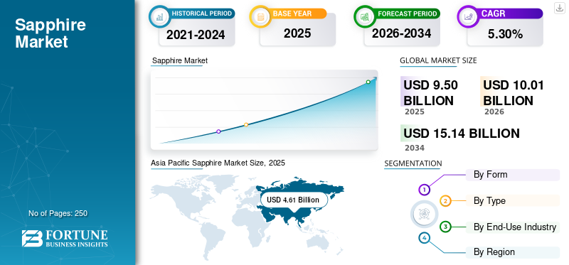
The global sapphire market size was valued at USD 9.50 billion in 2025. The market is projected to grow from USD 10.01 billion in 2026 to USD 15.14 billion by 2034, exhibiting a CAGR of 5.30% during the forecast period. Asia Pacific dominated the global market with a market share of 48.52% in 2025.
The global market is primarily driven by rising consumption in consumer electronics and semiconductor equipment, as its high hardness, thermal stability, and optical transparency make it suitable for LED substrates, camera lens covers, RF windows, and wafer carriers, thereby directly linking market growth to global electronics production growth.
- For instance, Topco Scientific recently unveiled Taiwan’s first large-size (12-inch) sapphire single-crystal substrates, showcasing them at SEMICON Taiwan 2025. These substrates are designed for advanced semiconductor and packaging applications, including LED and high-performance electronic components. This recent development highlights active commercial use and innovation around sapphire materials in the global semiconductor supply chain.
However, there are several key industry players, such as Rubicon Technology, LLC, Monocrystal, and Kyocera Corporation, operating in the market, are focusing on developing various innovative products to support the rising demand.
Download Free sample to learn more about this report.
Sapphire Market Key Takeaways
- 2025 Market Size: USD 9.50 billion
- 2026 Market Size: USD 10.01 billion
- 2034 Forecast Market Size: USD 15.14 billion
- CAGR: 5.30% from 2026–2034
- Asia Pacific dominated the sapphire market with a 48.52% share in 2025.
- Synthetic segment dominated the market in 2025 due to scalability and industrial applications.
- Electronics & energy segment is expected to hold a leading market position during the forecast period.
Asia Pacific
Asia Pacific reached USD 4.61 billion in 2025, holding 48.52% of the global market share.
North America
North America recorded USD 1.74 billion in 2024, driven by semiconductor and aerospace demand.
Europe
Europe is projected to reach USD 1.76 billion in 2026, supported by advanced manufacturing.
U.S.
The U.S. market is estimated at USD 1.79 billion in 2026, driven by defense and semiconductor applications.
Japan
Japan’s market is estimated at USD 0.85 billion in 2026, supported by optics and semiconductor industries.
Read More
SAPPHIRE MARKET TRENDS
Rising Adoption of Patterned Sapphire Substrates (PSS) is a Prominent Market Trend
The growing adoption of patterned sapphire substrates (PSS) represents a significant trend in the market, driven by the continuous push for high quality, higher performance and energy efficiency in LED and optoelectronic applications. PSS are wafers with micro- or nano-scale surface patterns that improve crystal quality during gallium nitride epitaxial growth and enhance light extraction efficiency. This technical advantage allows device manufacturers to achieve higher brightness levels while reducing power consumption, which is critical in meeting stringent global energy-efficiency regulations and sustainability targets.
As LED technologies evolve toward higher luminous efficacy and longer lifespans, demand for PSS is rising across general lighting, automotive lighting, display backlighting, and specialty illumination segments. From a market perspective, this trend is reshaping demand by shifting consumption from standard polished wafers to higher-value engineered substrates, thereby increasing revenue per wafer for suppliers. In addition, the growing complexity of PSS manufacturing is creating higher entry barriers, favoring technologically advanced producers with strong processing capabilities.
- For instance, Monocrystal, a leading global manufacturer, launched Ultra-Clean sapphire wafers designed for advanced applications including microLEDs and improved PSS yields, reflecting technological progress in wafer quality and processing.
Download Free sample to learn more about this report.
MARKET DYNAMICS
MARKET DRIVERS
Expanding LED and Optoelectronics Industry is Accelerating Market Growth
One of the most significant growth drivers of the global market is the expanding LED and optoelectronics industry, where it plays a critical functional role as a substrate material. Its high thermal stability, optical transparency, chemical resistance, and mechanical hardness make it particularly suitable for gallium nitride (GaN)–based LED fabrication, which dominates the global LED lighting and display ecosystem.
As governments and industries worldwide accelerate the transition toward energy-efficient lighting solutions, demand for high-brightness LEDs continues to grow across general lighting, automotive lighting, backlighting, and specialty illumination applications. Sapphire substrates are widely used in LED manufacturing as they provide a stable and compatible platform for GaN epitaxial growth, enabling higher luminous efficiency, longer device lifetimes, and improved thermal performance. This directly links LED production volumes and technology upgrades to growth in demand.
MARKET RESTRAINTS
High Production Cost and Energy-Intensive Manufacturing to Restrict Market Growth
The product manufacturing is an energy-intensive and time-consuming process, particularly for large-diameter boules and high-purity optical-grade material. Crystal growth techniques such as Kyropoulos and Czochralski require prolonged heating cycles, precise temperature control, and high electricity consumption, which significantly increases operating costs. In addition, post-growth processes including slicing, polishing, and surface patterning further add to production expenses.
This cost structure limits the product’s competitiveness against alternative materials such as tempered glass, Gorilla Glass, and other advanced ceramics, especially in price-sensitive applications such as mass-market consumer electronics. While the product offers superior hardness and durability, its higher cost often restricts its adoption to premium or performance-critical components rather than large-area applications.
MARKET OPPORTUNITIES
Rise of MicroLED Displays and Next-Generation Visual Technologies to Offer Market Growth Opportunities
MicroLEDs offer significant performance advantages over conventional LCD and OLED displays, including higher brightness, lower power consumption, longer lifespan, and superior contrast ratios. Sapphire substrates are widely regarded as a suitable platform for microLED epitaxial growth due to their high crystal stability, thermal resistance, and compatibility with gallium nitride (GaN).
As consumer electronics, automotive displays, augmented reality (AR), virtual reality (VR), and large-format commercial displays increasingly move toward microLED technology, demand for high-purity, defect-free wafers is expected to rise. Unlike traditional LED lighting, microLED production requires extremely tight quality tolerances, which increases value addition per wafer and creates opportunities for technologically advanced manufacturers.
MARKET CHALLENGES
Cost Competitiveness and Substitution Pressure to Pose a Critical Challenge to Market Growth
Sapphire offers superior hardness, thermal stability, and optical performance; however, its energy-intensive crystal growth, long production cycles, and complex processing requirements result in significantly higher costs compared to strengthened glass and other advanced ceramics. As a result, it struggles to achieve widespread adoption in high-volume, price-sensitive applications, particularly in consumer electronics.
Additionally, producers face challenges related to capacity utilization and pricing volatility, especially when LED demand fluctuates. Oversupply of mid-grade sapphire wafers in certain regions, particularly Asia, has led to price pressure and margin compression. At the same time, transitioning to higher-value segments such as microLED and aerospace optics requires substantial capital investment and long qualification cycles.
Segmentation Analysis
By Form
Increasing Wafers Adoption in LED Applications to Propel Segmental Growth
Based on the form, the market is divided into sapphire boules, wafers, and sheets.
The wafer segment is anticipated to account for the largest sapphire market share due to its direct integration into high-volume, high-value downstream industries, particularly LEDs and semiconductors. Wafers are increasingly used in semiconductor equipment and optoelectronics, including PSS, microLED development, RF components, and optical sensors. These applications require tight dimensional control, ultra-low defect density, and polished surfaces, all of which are achieved in the wafer form.
The sheets segment is anticipated to rise with a CAGR of 5.15% over the forecast period.
By Type
Scalability, Consistency, and Suitability For Industrial and Technological Applications Boosted Segment Growth
Based on type, the market is segmented into synthetic and natural.
In 2025, the synthetic segment dominated the global market due to its scalability, consistency, and suitability for technological and industrial applications. Synthetic product type is produced under controlled conditions using crystal growth methods such as Kyropoulos, Czochralski, and Edge-Defined Film-Fed Growth (EFG). These processes allow manufacturers to produce large, high-purity crystals with uniform optical and mechanical properties, which are essential for applications in LEDs, semiconductors, optics, aerospace, and medical devices.
Additionally, synthetic product type is more cost-effective at scale. While initial production is energy-intensive, synthetic processes allow yield optimization, recycling, and continuous improvement, reducing cost per unit over time
The natural segment is projected to grow at a CAGR of 4.55% over the forecast period.
By End-Use Industry
To know how our report can help streamline your business, Speak to Analyst
Electronics & Energy Segment to Lead Market Due to Ease of Administration
Based on the end-use industry, the market is segmented into aerospace & defense, medical, semiconductor equipment, electronics & energy, and others.
The electronics & energy segment is anticipated to witness a dominating market share over the forecast period. This dominance is primarily driven by high demand for LED lighting, displays, optical sensors, camera lenses, wearables, and power electronics. These wafers serve as substrates for GaN-based LEDs and are also used in protective covers and optical components. Growth is supported by energy-efficient lighting adoption, consumer electronics innovation, and renewable energy systems.
The semiconductor equipment segment is projected to grow at a highest CAGR of 6.03% over the forecast period.
Sapphire Market Regional Outlook
By region, the market is categorized into Europe, North America, Asia Pacific, Latin America, and the Middle East & Africa.
Asia Pacific
Asia Pacific Sapphire Market Size, 2025 (USD Billion)
To get more information on the regional analysis of this market, Download Free sample
Asia Pacific is estimated to reach USD 4.90 billion in 2026 and secure the position of the largest region in the market. Asia Pacific dominates the global market supported by its strong base in LED manufacturing, semiconductor fabrication, and consumer electronics production. China is the largest consumer of wafers, driven by extensive LED lighting and display manufacturing capacity, as well as ongoing investments in domestic semiconductor ecosystems.
Japan Sapphire Market
The Japan market in 2026 is estimated at around USD 0.85 billion, accounting for roughly 8.5% of global revenues. Japan contributes through high-purity sapphire components used in semiconductor equipment, optics, and medical devices.
China Sapphire Market
China’s market is projected to be one of the largest worldwide, with 2026 revenues estimated at around USD 2.02 billion, representing roughly 20.2% of global sales. China is the largest consumer of sapphire wafers, driven by extensive LED lighting and display manufacturing capacity, as well as ongoing investments in domestic semiconductor ecosystems. Government-led energy-efficiency programs and localization of supply chains further reinforce demand.
To know how our report can help streamline your business, Speak to Analyst
India Sapphire Market
The India market in 2026 is estimated at around USD 0.50 billion, accounting for roughly 5.0% of global revenues. India’s consumption is largely linked to LED lighting and electronics assembly. Government initiatives such as “Make in India”, expanding domestic electronics manufacturing, and large-scale adoption of LED lighting for infrastructure, residential, and commercial projects are indirectly supporting sapphire wafer demand through downstream LED usage.
North America
North America held the significant share in 2024, valuing at USD 1.74 billion. North America represents a technology-intensive and high-margin market, driven mainly by aerospace & defense, semiconductor equipment, and advanced optical applications. Demand in this region is also characterized by low-volume but high-value components, including optical windows, domes, and equipment parts that require extreme durability and precision
U.S. Sapphire Market
Based on North America’s strong contribution and the U.S. dominance within the region, the U.S. market can be analytically approximated at around USD 1.79 billion in 2026, accounting for roughly 17.8% of global sales. The United States leads regional demand due to strong defense spending, space exploration programs, and increasing investments in semiconductor manufacturing and research.
Europe
Europe is projected to record a growth rate of 4.50% in the coming years and reach a valuation of USD 1.76 billion by 2026. Europe’s market is shaped by precision engineering industries, particularly in aerospace, defense, medical devices, industrial optics, and luxury goods. Countries such as France, Germany, and the U.K. are key contributors, supported by strong R&D capabilities and advanced manufacturing infrastructure
U.K. Sapphire Market
The U.K. market in 2026 is estimated at around USD 0.14 billion, representing roughly 1.4% of global revenues.
Germany Sapphire Market
Germany’s market is projected to reach approximately USD 0.45 billion in 2026, equivalent to around 4.5% of global sales.
Latin America and Middle East & Africa
Latin America and the Middle East & Africa regions are expected to witness moderate growth in this market space during the forecast period. The Latin America market is set to reach a valuation of USD 0.50 billion in 2026. In Latin America, the demand is primarily linked to electronics assembly, research applications, and luxury goods, rather than upstream manufacturing. The region has limited LED wafer fabrication and semiconductor production capacity, which restricts large-scale usage.
The Middle East & Africa reached a value of USD 0.09 billion in 2025.
GCC Sapphire Market
The GCC market is projected to reach around USD 0.35 billion in 2026, representing roughly 3.5% of global revenues.
COMPETITIVE LANDSCAPE
Key Industry Players
Focus On Innovations By Key Players To Propel Market Progress
The global market is moderately consolidated, characterized by the presence of a limited number of large, technologically advanced manufacturers such as Rubicon Technology, Monocrystal, and Kyocera Corporation LLC and a fragmented base of regional and niche suppliers. Competition is shaped primarily by crystal growth capability, wafer size scalability, purity levels, processing technology, and long-term relationships with end-use industries such as LEDs, semiconductors, aerospace, and medical devices.
Other notable players in the global market include Orbray Co. Ltd, Swiss Jewel Company, and SCHOTT AG. These companies are expected to prioritize new product launches and collaborations to increase their global market share during the forecast period.
LIST OF KEY SAPPHIRE COMPANIES PROFILED
- Rubicon Technology, LLC (U.S.)
- Monocrystal (Russia)
- Kyocera Corporation (Japan)
- Orbray Co. Ltd (Japan)
- Chatham Created Gems & Diamonds (U.S.)
- Swiss Jewel Company (Switzerland)
- Crystalwise Technology (Taiwan)
- SCHOTT AG (Germany)
- Topco Scientific (Taiwan)
KEY INDUSTRY DEVELOPMENTS
- June 2025: Kyocera participated in World of Quantum 2025 taking place from June 24-27 in Munich, Germany. The company unveiled its innovative material solutions that are accelerating the progression of quantum technologies across various industries, including finance, medicine, automotive, chemical sectors, and quantum sensing applications. The products include sapphire wafer, window and ceramic feedthrough.
- November 2022: Orbray Co. Ltd With its precision processing technology, launched a new line up large 12-inch high quality sapphire wafer. The company began test sales of large-sized 12-inch(Φ300mm) sapphire wafers.
- February 2024: Chatham Created Gems & Diamonds has introduced lab-grown purple sapphire as a premium alternative to the traditional February birthstone, amethyst.
REPORT COVERAGE
Request for Customization to gain extensive market insights.
Report Scope & Segmentation
|
ATTRIBUTE |
DETAILS |
|
Study Period |
2021-2034 |
|
Base Year |
2025 |
|
Estimated Year |
2026 |
|
Forecast Period |
2026-2034 |
|
Historical Period |
2021-2024 |
|
Growth Rate |
CAGR of 5.30% from 2026-2034 |
|
Unit |
Value (USD Billion) |
|
Segmentation |
By Form, Type, End-Use Industry, and Region |
|
By Form |
· Sapphire Boules · Wafers · Sheets |
|
By Type |
· Synthetic · Natural |
|
By End-Use Industry |
· Aerospace & Defense · Medical · Semiconductor Equipment · Electronics & Energy · Others |
|
By Region |
· North America (By Form, Type, End-Use Industry, and Country) o U.S. (By End-Use Industry) o Canada (By End-Use Industry) · Europe (By Form, Type, End-Use Industry, and Country) o Germany (By End-Use Industry) o U.K. (By End-Use Industry) o France (By End-Use Industry) o Italy (By End-Use Industry) o Rest of Europe (By End-Use Industry) · Asia Pacific (By Form, Type, End-Use Industry, and Country) o China (By End-Use Industry) o Japan (By End-Use Industry) o India (By End-Use Industry) o South Korea (By End-Use Industry) o Rest of Asia Pacific · Latin America (By Form, Type, End-Use Industry, and Country) o Brazil (By End-Use Industry) o Mexico (By End-Use Industry) o Rest of Latin America (By End-Use Industry) · Middle East & Africa (By Form, Type, End-Use Industry, and Country) o GCC (By End-Use Industry) o South Africa (By End-Use Industry) o Rest of the Middle East & Africa (By End-Use Industry) |
Frequently Asked Questions
According to Fortune Business Insights, the global market value stood at USD 9.50 billion in 2025 and is projected to reach USD 15.14 billion by 2034
In 2025, the market value stood at USD 4.6 billion.
The market is expected to exhibit a CAGR of 5.30% during the forecast period.
By form, the wafers segment is expected to lead the market.
The increasing demand from LED and Optoelectronics industry is driving market expansion.
Rubicon Technology, Monocrystal, and Kyocera Corporation LLC are the major players in the global market.
Asia Pacific dominated the market in 2025.


- 2021-2034
- 2025
- 2021-2024
- 250
Get 30-60 hrs Free Customization
Expand Regional and Country Coverage, Segments Analysis, Company Profiles, Competitive Benchmarking, and End-user Insights.
Related Reports
-
US +1 833 909 2966 ( Toll Free )
-
Get In Touch With Us