Silicon Wafers Market Size, Share & Industry Analysis, By Wafer Size (300 mm, 200 mm, and Up to 150mm), By End Use (Consumer Electronics, Computing & Data Infrastructure, Telecommunications, Automotive, Industrial, Healthcare, and Others), and Regional Forecast, 2026-2034
 Download Free Sample
Silicon Wafers Market Size and Future Outlook
 Listen to Audio Version
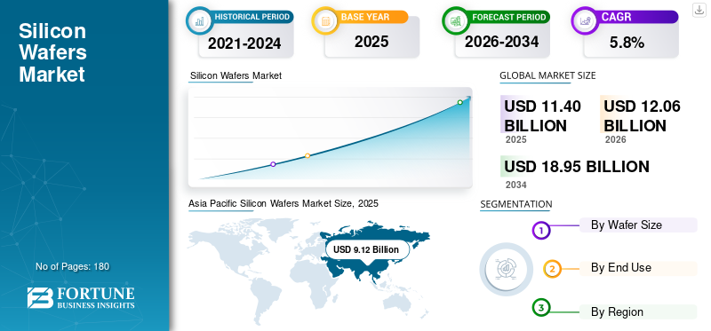
The global silicon wafers market size was valued at USD 11.40 billion in 2025 and is projected to grow from USD 12.06 billion in 2026 to USD 18.95 billion by 2034, exhibiting a CAGR of 5.8% during the forecast period. Asia Pacific dominated the silicon wafers market with a market share of 80.00% in 2025.
Silicon wafers are highly engineered semiconductor substrates used in the fabrication of integrated circuits, discrete devices, power components, sensors, and optoelectronic products. They serve as the foundational platform on which semiconductor devices are built through successive processes such as deposition, lithography, etching, doping, and packaging. The rising deployment of artificial intelligence infrastructure, 5G communication systems, electric vehicles, advanced driver-assistance systems, industrial automation, and high-performance consumer electronics is driving the global market. AI accelerators, high-bandwidth memory, automotive microcontrollers, power semiconductors, image sensors, and advanced logic chips require wafers with tighter dimensional tolerances, better crystal quality, and compatibility with increasingly complex node architectures. Therefore, market growth is supported not only by rising semiconductor production volumes but also by the industry's transition to larger-diameter wafers.
The global market is shaped by a concentrated group of established silicon wafer manufacturers with strong capabilities in crystal growth, wafer slicing, polishing, epitaxial deposition, and defect-control technologies. Major market leaders include Shin-Etsu Handotai (SEH), SUMCO Corporation, GlobalWafers Co., Ltd., Siltronic AG, and SK Siltron. These companies hold strong positions in the global semiconductor supply chain due to their expertise in high-purity substrate manufacturing, large-diameter wafer production, and consistent supply to leading chipmakers.
Download Free sample to learn more about this report.
SILICON WAFERS MARKET KEY TAKEAWAYS
 Global Market Size & Forecast
- 2025 Market Size: USD 11.40 billion
- 2026 Market Size: USD 12.06 billion
- 2034 Forecast Market Size: USD 18.95 billion
- CAGR: 5.80% from 2026–2034
 Market Share
- Asia Pacific dominated the market with an 80.00% share in 2025.
- The 300 mm segment is expected to hold the largest market share in 2026.
- The Consumer Electronics segment is expected to hold the largest market share in 2026.
 Key Regional Highlights
Asia Pacific
The market reached USD 9.12 billion in 2025 and is projected to witness steady growth at a 5.90% CAGR through the forecast period.
North America
The market reached USD 1.25 billion in 2025 and is projected to grow at a 5.60% CAGR through the forecast period.
Europe
The market reached USD 0.91 billion in 2025 and is projected to grow at a 5.10% CAGR through the forecast period.
U.S.
The market is projected to reach USD 1.26 billion by 2026.
Japan
The market is projected to witness steady growth through the forecast period.
Read More

SILICON WAFERS MARKET TRENDS
Growing Demand for Specialty Wafers and Advanced Chip Fabrication to Accelerate Product Adoption
Growing demand for specialty wafers and advanced chip fabrication is emerging as a key trend in the global market. While standard polished wafers continue to account for a significant share of the semiconductor industry, demand is increasingly shifting toward higher-value products such as epitaxial wafers, silicon-on-insulator wafers, and wafers engineered for power devices, sensors, MEMS, and advanced logic applications. This trend is being supported by the growing complexity of semiconductor architectures used in artificial intelligence processors, high-performance computing, image sensing, and automotive electronics. In addition, the transition toward smaller process nodes, advanced packaging, and heterogeneous integration is increasing the need for wafers with tighter specifications, lower defect density, and better surface uniformity. Therefore, product adoption is increasingly driven by performance requirements rather than by volume demand alone.
MARKET DYNAMICS
MARKET DRIVERS
Download Free sample to learn more about this report.
Rising Semiconductor Demand from AI and 5G Infrastructure to Drive Market Growth
Rising semiconductor demand from emerging technologies, such as artificial intelligence and 5G infrastructure, is a major driver for market growth. AI servers, accelerators, GPUs, high-bandwidth memory, and edge computing systems require increasingly advanced semiconductor devices, all of which depend on high-quality silicon wafer substrates. At the same time, the continued rollout of 5G networks is supporting wafer demand through higher production of RF chips, processors, networking hardware, and telecom base-station components. These applications require greater chip density, faster processing capabilities, and improved energy efficiency, thereby increasing the need for advanced wafer solutions compatible with leading-edge fabrication. Moreover, the expansion of hyperscale data centers and connected-device ecosystems is further supporting semiconductor output globally. Hence, the rising deployment of AI and 5G technologies is set to drive the global silicon wafers market growth.
- For instance, according to 5G Americas, 5G adoption is experiencing explosive growth, with global connections surpassed 2.25 billion in April 2025, expanding 4 times faster than 4G.
MARKET RESTRAINTS
High Capital Intensity and Complex Manufacturing Requirements Limiting New Capacity Development
High capital intensity and complex manufacturing requirements remain major restraints in the global silicon wafer market. Silicon wafer production involves highly specialized processes, including polysilicon purification, crystal pulling, ingot shaping, wafer slicing, polishing, cleaning, and epitaxial deposition, each of which requires advanced equipment, strict process control, and significant technical expertise. Establishing new production capacity, particularly for 300 mm wafers and advanced specifications, requires substantial investment and long lead times before commercial output can be stabilized. In addition, manufacturers must maintain extremely low defect rates, high flatness standards, and consistent quality across large-scale production, further increasing operational complexity. These barriers limit the pace at which new entrants can expand in the market and can delay supply response during periods of strong semiconductor demand. Therefore, capacity expansion remains structurally constrained.
MARKET OPPORTUNITIES
Rising Demand for Power Electronics and Automotive Chips Opening New Avenues in Market
Rising demand for power electronics and automotive chips is creating significant growth opportunities in the global market. The automotive industry is transitioning from Internal Combustion Engines (ICE) to electric and hybrid vehicles, creating unprecedented demand for silicon wafers as these vehicles require two to three times as many semiconductor chips as traditional ICE vehicles. In addition, renewable energy systems require a growing volume of power semiconductors, analog devices, and control chips, all of which depend on reliable wafer substrates. This is expanding the addressable market for silicon wafers beyond traditional computing and consumer electronics segments. In addition, many automotive and power applications require specialty wafer characteristics tailored for performance, durability, and thermal stability. As electrification and vehicle intelligence continue to expand globally, wafer suppliers are gaining new opportunities to strengthen their positions in high-value, long-term growth applications.
Segmentation Analysis
By Wafer Size
300 mm Segment Dominates Market Owing to their Critical Role in Advanced Semiconductor Manufacturing
Based on wafer size, the market is segmented into 300 mm, 200 mm, and up to 150 mm.
The 300 mm segment accounts for the largest share of the global market due to their extensive use in advanced semiconductor manufacturing across logic chips, memory devices, image sensors, and high-performance computing applications. These wafers enable greater chip output per fabrication cycle, better economies of scale, and improved manufacturing efficiency compared to smaller wafer formats. Their adoption remains particularly strong in leading-edge fabs serving artificial intelligence, cloud infrastructure, consumer electronics, and automotive semiconductor demand.
The 200 mm wafers continue to hold a significant position in the market, supported by their broad use in analog semiconductors, power devices, MEMS, sensors, and discrete components. Unlike leading-edge digital chips that are increasingly concentrated on 300 mm platforms, many industrial, automotive, and embedded applications still rely on mature-node production where 200 mm lines remain cost-effective and technically suitable. Therefore, the segment is expected to maintain steady momentum and expand at a 5.3% CAGR from 2026 to 2034, supported by resilient demand from automotive electronics, industrial equipment, and specialty semiconductor applications.
Up to 150 mm wafers represent a comparatively smaller but still relevant portion of the global market, primarily serving legacy semiconductor production, research applications, certain discrete devices, and niche industrial uses. These wafers are typically associated with older fabrication infrastructure and lower-volume applications where migration to larger wafer formats is not always economically justified. Demand remains visible in selected power components, optoelectronics, academic research, and specialized device categories with limited scale requirements. However, growth prospects are relatively modest, as the industry increasingly favors larger diameters to improve productivity and cost efficiency. Hence, the segment is projected to grow at a CAGR of 2.4% from 2026 to 2034, reflecting its mature and specialized market positioning.
By End Use
Consumer Electronics Segment Dominated Market Backed by Broad Semiconductor Consumption across High-Volume Devices
Based on end use, the market is segmented into consumer electronics, computing & data centers, automotive, industrial, telecommunications, healthcare, and others.
To know how our report can help streamline your business, Speak to Analyst
The consumer electronics segment accounted for the largest global silicon wafers market share in 2025, driven by the massive semiconductor requirements of smartphones, tablets, laptops, wearables, smart home products, gaming devices, and other connected electronics. This segment benefits from large-scale unit shipments, frequent product upgrades, and rising integration of advanced chips for processing, memory, sensing, connectivity, and power management. Moreover, IoT devices are exponentially increasing the demand for silicon wafers by requiring vast amounts of sensors, microcontrollers, and connectivity chips (5G, Bluetooth) for smart, interconnected electronics. Silicon wafers remain fundamental to the production of these semiconductor components, making consumer electronics a major driver for global wafer demand.
The computing & data centers segment are emerging as one of the most dynamic end-use segments in the market, supported by expanding demand for AI accelerators, CPUs, GPUs, memory chips, and networking semiconductors. Growth in hyperscale cloud infrastructure, enterprise digitalization, and high-performance computing is driving increased demand for advanced semiconductor manufacturing, particularly for high-value logic and memory applications. As artificial intelligence deployment continues to accelerate globally, this segment is expected to record robust expansion at a CAGR of 6.5% from 2026 to 2034, making it one of the fastest-growing demand centers in the market.
The industrial segment is set to generate steady demand for silicon wafers through their use in automation equipment, industrial controls, robotics, power systems, sensors, and factory digitization technologies. The adoption of Industry 4.0 frameworks, intelligent monitoring systems, and energy-efficient control solutions continues to create stable demand for analog, embedded, and power semiconductor devices. As manufacturing systems become more connected and data-driven, silicon wafer consumption in this segment is expected to rise at a CAGR of 5.5% from 2026 to 2034, reflecting durable medium-term growth fundamentals.
Silicon Wafers Market Regional Outlook
By geography, the market is segmented into North America, Europe, Asia Pacific, and the rest of the world.
Asia Pacific
Asia Pacific Silicon Wafers Market Size, 2025 (USD Billion)
To get more information on the regional analysis of this market, Download Free sample
Asia Pacific dominated the global silicon wafer market in 2025, reaching USD 9.12 billion, and is expected to maintain its leadership in the coming years, expanding at a CAGR of 5.9% through the forecast period. The region accounts for the majority of global silicon wafer demand due to its dense concentration of semiconductor fabrication capacity across China, Taiwan, South Korea, Japan, and India. Strong manufacturing ecosystems, large-scale electronics production, and continued investments in logic, memory, foundry, and power semiconductor capacity continue to support regional wafer consumption. In addition, the growing need for wafers across artificial intelligence chips, consumer electronics, automotive semiconductors, and telecom devices is reinforcing the Asia Pacific’s position as the core demand center in the global market.
China Silicon Wafers Market
China is estimated to account for approximately USD 3.38 billion in 2026, representing around 28.0% of global demand. The country remains the largest individual market due to its broad semiconductor manufacturing base, expanding domestic wafer fabrication ecosystem, and strong policy support for greater self-reliance in semiconductor materials and components. Continued investments across mature-node foundries, power semiconductor lines, memory projects, and local electronics manufacturing are supporting demand.
To know how our report can help streamline your business, Speak to Analyst
Taiwan Silicon Wafers Market
Taiwan’s market is set to reach USD 2.43 billion in 2026, accounting for nearly 20.1% of global revenues, making it one of the most significant country-level markets in the global industry. The market is strongly supported by Taiwan’s central role in the semiconductor value chain, particularly in advanced logic, foundry manufacturing, and high-performance chip production.
North America
North America reached USD 1.25 billion in 2025 and is projected to grow at a CAGR of 5.6% through the forecast period. The region is supported by a strong semiconductor ecosystem comprising advanced chip designers, integrated device manufacturers, and increasing domestic fabrication investments aimed at improving supply chain resilience. Demand for silicon wafers is being driven by expansion in high-performance computing, artificial intelligence processors, defense electronics, automotive semiconductors, and industrial chips.
U.S. Silicon Wafers Market
The U.S. market is set to reach USD 1.26 billion in 2026, accounting for roughly 10.4% of global revenues. The country’s position is supported by its strong semiconductor design base, rising investments in domestic fabrication facilities, and growing demand from data centers, AI infrastructure, aerospace electronics, and automotive semiconductor applications.
Europe
Europe reached USD 0.91 billion in 2025, growing at a CAGR of 5.1% through the forecast period. The region represents a technically strong but relatively specialized silicon wafer demand center, with semiconductor activity concentrated more in automotive electronics, industrial automation, sensors, and power devices rather than in leading-edge logic manufacturing.
Germany Silicon Wafers Market
The German market is set to reach USD 0.32 billion in 2026, representing around 2.6% of global demand. The country benefits from its strong position in automotive electronics, industrial semiconductors, and power device manufacturing, all of which support stable silicon wafer consumption.
U.K. Silicon Wafers Market
The U.K. market is set to reach USD 0.21 billion in 2026, accounting for about 1.8% of global revenues. Unlike larger manufacturing-driven markets, the U.K.’s silicon wafer demand is supported more selectively by semiconductor design activity, compound and specialty electronics, research-intensive applications, and niche industrial technologies.
Rest of World
The rest of world region reached USD 0.11 billion in 2025, expanding at a CAGR of 4.5% through the projected period. This region includes smaller and emerging semiconductor markets across Latin America, the Middle East, and other developing electronics manufacturing locations. Demand is primarily associated with limited-scale semiconductor activity, industrial electronics, research applications, and selected downstream device manufacturing rather than large commercial wafer fabrication hubs.
COMPETITIVE LANDSCAPE
Key Industry Players
Capacity Expansion and Advanced Wafer Technology Investments Reinforce Competitive Positioning
The global silicon wafer market is highly consolidated, with competition led by a small group of large-scale manufacturers that combine crystal-growth expertise, precision wafer processing, advanced polishing capabilities, and long-term relationships with semiconductor fabs. Leading companies in the market are Shin-Etsu Handotai (SEH), SUMCO Corporation, GlobalWafers Co., Ltd., Siltronic AG, and SK Siltron, who have maintained strong market positions through broad product portfolios across 300 mm, 200 mm, and specialty wafers, along with high consistency in quality and supply reliability. Companies are increasingly directing investments toward 300 mm capacity expansion, specialty wafer development, and localized manufacturing footprints to support advanced chip production and improve supply-chain resilience. At the same time, integrated “megasite” strategies and technology upgrades in epitaxial and polished wafers are strengthening competitive differentiation. Therefore, market evolution is increasingly being shaped by scale-backed expansion and technology-focused investment strategies.
LIST OF KEY SILICON WAFERS COMPANIES PROFILED
- Shin-Etsu Chemical Co., Ltd. (Japan)
- SUMCO Corporation (Japan)
- GlobalWafers Co., Ltd. (Taiwan)
- Siltronic AG (Germany)
- SK Siltron Co., Ltd. (South Korea)
- Soitec S.A. (France)
- Okmetic Oy (Finland)
- Wafer Works Corporation (Taiwan)
- RS Technologies Co., Ltd. (Japan)
- National Silicon Industry Group (NSIG) (China)
KEY INDUSTRY DEVELOPMENTS
- May 2025: GlobalWafers officially opened its new 300 mm silicon wafer facility in Sherman, Texas, representing an initial investment of USD 3.5 billion. At the inauguration, the company also announced plans to invest an additional USD 4.0 billion, taking the total planned investment at the site to USD 7.5 billion.
- June 2024: Siltronic inaugurated its new wafer fab in Singapore, describing it as one of the world’s most advanced and cost-efficient facilities. The company stated that the fab was commissioned at the beginning of 2024 and would be ramped to full capacity over several years.
- November 2023: Siltronic announced the production of the first wafers at its new 300 mm fab in Singapore. The company said the milestone marked a key step in the strategic expansion of its global production network, with the project remaining on schedule and on budget.
- September 2022: SK Siltron approved an additional investment of USD 0.69 billion to expand facilities for 300 mm silicon wafer production in Gumi, South Korea. The company noted that this followed an earlier new fab investment of more than USD 0.84 billion, making it one of the largest wafer capacity expansion efforts in the region.
REPORT COVERAGE
The global silicon wafers market analysis provides an in-depth study of market size & forecast across all market segments included in the report. It includes details on the market dynamics and market trends expected to drive the market during the forecast period. It offers information on technological advancements, new product launches, key industry developments, and partnerships, mergers & acquisitions. The market research report also encompasses a detailed competitive landscape, including market share and profiles of key operating players.
Request for Customization to gain extensive market insights.
Report Scope & Segmentation
| ATTRIBUTE | DETAILS |
| Study Period | 2021-2034 |
| Base Year | 2025 |
| Estimated Year | 2026 |
| Forecast Period | 2026-2034 |
| Historical Period | 2021-2024 |
| Growth Rate | CAGR of 5.8% from 2026-2034 |
| Unit | Value (USD Billion) |
| Segmentation | By Wafer Size, End Use, and Region |
| By Wafer Size |
|
| By End Use |
|
| By Region |
|
Frequently Asked Questions
Fortune Business Insights says that the global market size was valued at USD 11.40 billion in 2025 and is projected to reach USD 18.95 billion by 2034.
In 2025, the Asia Pacific’s market value stood at USD 9.12 billion.
Recording a CAGR of 5.8%, the market is slated to exhibit steady growth during the forecast period of 2026-2034.
The consumer electronics led the end use segment.
Rising semiconductor demand from AI and 5G infrastructure is expected to drive market growth.
Shin-Etsu Handotai (SEH), SUMCO Corporation, GlobalWafers Co., Ltd., Siltronic AG, and SK Siltron are the top players in the market.
Asia Pacific held the highest market share in 2025.
The growing demand for specialty wafers and advanced chip fabrication is expected to favor product adoption.

- 2021-2034
- 2025
- 2021-2024
- 180
Get 30-60 hrs Free Customization
Expand Regional and Country Coverage, Segments Analysis, Company Profiles, Competitive Benchmarking, and End-user Insights.


















Related Reports
-
US +1 833 909 2966 ( Toll Free )
-
Get In Touch With Us