Wafer Inspection Equipment Market Size, Share & Industry Analysis, By Inspection Type (Patterned Wafer Inspection, Unpatterned Wafer Inspection, Mask Inspection, and Others), By Technology (Optical Inspection, E-Beam Inspection, X-Ray Inspection, and Others), By Application (Foundries, IDMs, Memory Manufacturers, and Others), By Wafer Size (150 mm, 200 mm, 300 mm, and Others), and Regional Forecast, 2026–2034
Wafer Inspection Equipment Market Size and Future Outlook
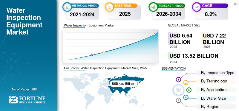
The global wafer inspection equipment market size was valued at USD 6.64 billion in 2025. The market is projected to grow from USD 7.22 billion in 2026 to USD 13.52 billion by 2034, exhibiting a CAGR of 8.2% during the forecast period. Asia Pacific dominated the wafer inspection equipment market with a market share of 67.77% in 2025.
The market is witnessing steady expansion as semiconductor manufacturers increasingly invest in advanced inspection tools to improve yield, enhance process control, and support production of high-performance chips. The market growth is driven by the rising demand for advanced semiconductors used in electronic devices, artificial intelligence, automotive electronics, and data centers. The increasing complexity of semiconductor manufacturing is significantly contributing to the market growth, as manufacturers require highly accurate defect detection and process monitoring solutions. Wafer inspection equipment plays a critical role in identifying defects and ensuring manufacturing precision during semiconductor fabrication. Key players such as KLA Corporation, Applied Materials, and Hitachi High-Tech are actively investing in advanced optical and e-beam inspection technologies to improve defect detection and strengthen their market position. Over the long term, the increasing complexity of semiconductor architectures and the growing adoption of advanced process nodes are expected to support market expansion.
Download Free sample to learn more about this report.
Global Wafer Inspection Equipment Market KEY TAKEAWAYS
- 2025 Market Size: USD 6.64 billion
- 2026 Market Size: USD 7.22 billion
- 2034 Forecast Market Size: USD 13.52 billion
- CAGR: 8.2% from 2026–2034
- Asia Pacific dominated the global market with a 67.77% share and a market value of USD 4.50 billion in 2025.
- The patterned wafer inspection segment accounted for the highest market share in 2025.
- The optical inspection segment accounted for the highest market share in 2025.
Asia Pacific
The region dominated the market with a value of USD 4.50 billion in 2025.
North America
The market is projected to reach USD 1.28 billion in 2026.
Europe
The market is estimated to reach USD 0.70 billion in 2026.
U.S.
The market is estimated to reach USD 0.96 billion in 2026.
Japan
The market is estimated to reach USD 0.85 billion in 2026, accounting for roughly 11.7% of global revenue.
Read More
WAFER INSPECTION EQUIPMENT MARKET TRENDS
Increasing Semiconductor Complexity to Drive the Adoption of Advanced Inspection Technologies
The market is experiencing a growing demand for advanced inspection technologies as semiconductor devices continue to become smaller, more complex, and highly integrated. Manufacturers are increasingly adopting high-resolution optical and e-beam inspection systems to detect microscopic defects and improve production yield. The transition toward advanced process nodes, 3D architectures, and heterogeneous integration is further increasing the importance of precision inspection solutions. Additionally, the integration of AI and data analytics into inspection platforms is enabling faster defect classification and process optimization, supporting improved manufacturing efficiency across semiconductor fabrication facilities.
- For instance, KLA Corporation has continued expanding its advanced wafer inspection portfolio to support defect detection requirements for next-generation semiconductor manufacturing.
MARKET DYNAMICS
MARKET DRIVERS
Download Free sample to learn more about this report.
Rising Demand for Advanced Semiconductors and Yield Optimization to Drive Market Growth
The increasing demand for high-performance semiconductors and the need to improve manufacturing yield are major market drivers. Semiconductor manufacturers are investing heavily in advanced inspection systems to identify defects at early stages of production and minimize yield loss. The rapid adoption of AI, 5G, automotive electronics, and high-performance computing is further increasing the demand for advanced chips, driving the need for high-precision inspection technologies. Additionally, shrinking semiconductor geometries and increasing wafer complexity are making inspection systems essential for maintaining manufacturing quality and efficiency.
MARKET RESTRAINTS
High Equipment Cost and Technological Complexity to Limit Product Adoption
Despite strong growth potential, the market faces challenges due to the high cost associated with advanced wafer inspection equipment. Technologies such as e-beam and high-resolution optical inspection systems require significant investment and technical expertise. Additionally, increasing semiconductor complexity demands continuous upgrades in inspection capabilities, raising operational and maintenance costs. Small and mid-sized semiconductor manufacturers may face difficulties in adopting advanced inspection systems due to financial and technical constraints, limiting broader market penetration.
MARKET OPPORTUNITIES
Expansion of Advanced Process Nodes and AI-Driven Inspection Systems to Create Growth Opportunities
The increasing transition toward advanced semiconductor process nodes and AI-driven manufacturing is creating significant opportunities for market players. Manufacturers are adopting intelligent inspection systems capable of real-time defect analysis, predictive monitoring, and automated process optimization. The growing deployment of advanced packaging technologies and 3D semiconductor architectures is also increasing the demand for high-precision inspection solutions. Furthermore, the integration of machine learning and automation into inspection equipment is enabling faster throughput and improved defect detection accuracy, supporting long-term wafer inspection equipment market growth.
- For instance, semiconductor equipment manufacturers are increasingly integrating AI-based analytics into wafer inspection platforms to improve yield management and process efficiency.
Segmentation Analysis
By Inspection Type
Patterned Wafer Inspection Segment Held the Largest Share Due to High Demand for Advanced Process Monitoring
Based on inspection type, the market is divided into patterned wafer inspection, unpatterned wafer inspection, mask inspection, and others.
In 2025, the patterned wafer inspection segment accounted for the highest wafer inspection equipment market share due to the increasing complexity of semiconductor devices and the need for precise defect detection during advanced manufacturing processes. Patterned wafer inspection systems are critical for identifying defects in integrated circuit patterns and ensuring manufacturing yield. The growing adoption of advanced process nodes and high-density chip architectures is further driving the demand for high-resolution inspection technologies. Additionally, semiconductor foundries are increasingly investing in advanced patterned inspection systems to maintain process control and product quality.
The mask wafer inspection segment is anticipated to rise at a CAGR of 8.0% over the forecast period.
To know how our report can help streamline your business, Speak to Analyst
By Technology
Optical Inspection Segment Held the Largest Share Owing to Non-destructive Defect Detection across Semiconductor Manufacturing
Based on technology, the market is segmented into optical inspection, e-beam inspection, X-ray inspection, and others.
In 2025, the optical inspection segment accounted for the highest market share due to its ability to provide high-speed and non-destructive defect detection across semiconductor manufacturing processes. Optical inspection systems are widely adopted as they offer high throughput and cost-effective inspection capabilities for various wafer types and process nodes. Continuous advancements in imaging resolution and AI-driven analytics are further improving the efficiency and accuracy of optical inspection technologies, supporting segment dominance.
The e-beam inspection segment is expected to grow at a CAGR of 8.6% over the forecast period.
By Application
Foundries Segment Held the Largest Share Driven by Large-Scale Semiconductor Manufacturing Activities
Based on application, the market is segmented into foundries, IDMs, memory manufacturers, and others.
In 2025, the foundries segment accounted for the highest market share due to large-scale semiconductor manufacturing operations and increasing demand for advanced process control solutions. Foundries require high-performance inspection equipment to ensure yield optimization and maintain production quality across advanced semiconductor nodes. The rapid growth of fabless semiconductor companies and increasing outsourcing of chip manufacturing are further driving investments in advanced wafer inspection systems within foundries.
The memory manufacturers segment is expected to grow at a CAGR of 8.3% over the forecast period.
By Wafer Size
300 mm Segment Dominated the Market due to Widespread Adoption in Advanced Semiconductor Manufacturing
Based on wafer size, the market is segmented into 150 mm, 200 mm, 300 mm, and others.
In 2025, the 300 mm segment accounted for the highest market share due to its widespread use in advanced semiconductor manufacturing processes. Semiconductor manufacturers prefer 300 mm wafers as they offer higher production efficiency and lower cost per chip compared to smaller wafer sizes. The increasing production of advanced logic and memory devices is further driving the demand for inspection systems optimized for 300 mm wafer manufacturing. Additionally, ongoing investments in advanced fabrication facilities are supporting the continued growth of this segment.
The 200 mm segment is expected to grow at a CAGR of 7.9% over the forecast period.
Wafer Inspection Equipment Market Regional Outlook
By geography, the market is categorized into Europe, North America, Asia Pacific, South America, and the Middle East & Africa.
Asia Pacific
Asia Pacific Wafer Inspection Equipment Market Size, 2025 (USD Billion)
To get more information on the regional analysis of this market, Download Free sample
Asia Pacific held the dominant position in the market in 2024 and continued to lead in 2025, with a market valuation of USD 4.50 billion. The region’s dominance is driven by the presence of major semiconductor manufacturing hubs, increasing investments in advanced fabrication facilities, and strong demand for consumer electronics. Countries such as China, Taiwan, South Korea, and Japan are heavily investing in semiconductor production and process optimization technologies, supporting the strong product demand.
Japan Wafer Inspection Equipment Market
The Japan market is estimated at around USD 0.85 billion in 2026, accounting for roughly 11.7% of the global revenue.
China Wafer Inspection Equipment Market
The China market is estimated to reach around USD 1.62 billion in 2026, accounting for roughly 22.4% of global revenue.
India Wafer Inspection Equipment Market
The India market is estimated to touch around USD 0.34 billion in 2026, accounting for roughly 4.6% of the global market.
North America
The North America market is projected to reach USD 1.28 billion in 2026. North America holds a significant share driven by the strong presence of semiconductor technology companies and increasing investments in advanced chip manufacturing and R&D activities.
U.S. Wafer Inspection Equipment Market
The U.S. market is estimated to touch around USD 0.96 billion in 2026. The U.S. market is driven by increasing investments in semiconductor manufacturing, advanced process technologies, and growing demand for high-performance chips across industries.
Europe
The Europe market is estimated to touch around USD 0.70 billion in 2026. Europe demonstrates steady growth supported by increasing semiconductor investments and growing focus on strengthening regional chip manufacturing capabilities.
U.K. Wafer Inspection Equipment Market
The U.K. market is estimated to reach around USD 0.11 billion in 2026, representing roughly 1.6% of global revenues.
Germany Wafer Inspection Equipment Market
The Germany market is projected to reach USD 0.22 billion in 2026, equivalent to around 3.1% of global sales.
South America and Middle East & Africa
The South America and the Middle East & Africa markets are anticipated to experience moderate growth over the forecast period. South America is projected to reach a market value of USD 0.20 billion by 2026. South America is expected to witness gradual growth during the forecast period, supported by increasing electronics demand and industrial development. Meanwhile, the Middle East & Africa market is expected to attain a value of USD 0.13 billion by 2026. The Middle East & Africa region is projected to grow steadily, supported by rising investments in technology infrastructure and semiconductor-related industries.
GCC Wafer Inspection Equipment Market
The GCC market is projected to reach around USD 0.06 billion in 2026, representing roughly 0.8% of the global market.
COMPETITIVE LANDSCAPE
Key Industry Players
Key Players Focus on Advanced Defect Detection and AI-Integrated Inspection Technologies to Strengthen Market Position
The wafer inspection equipment market is moderately consolidated, with key players focusing on advanced imaging technologies, AI integration, and high-resolution inspection capabilities to strengthen their market position. Companies such as KLA Corporation, Applied Materials, Hitachi High-Tech, and ASML are investing heavily in next-generation inspection systems to support advanced semiconductor manufacturing. Market participants are emphasizing innovation, automation, and process optimization to improve yield management and manufacturing efficiency. Strategic collaborations, product innovation, and expansion of semiconductor manufacturing capabilities are further intensifying competition in the market.
LIST OF KEY WAFER INSPECTION EQUIPMENT COMPANIES PROFILED
- KLA Corporation (U.S.)
- Applied Materials, Inc. (U.S.)
- Hitachi High-Tech Corporation (Japan)
- ASML Holding N.V. (Netherlands)
- Tokyo Electron Limited (Japan)
- Onto Innovation Inc. (U.S.)
- Camtek Ltd. (Israel)
- Lasertec Corporation (Japan)
- SCREEN Holdings Co., Ltd. (Japan)
- Nikon Corporation (Japan)
KEY INDUSTRY DEVELOPMENTS
- October 2025: Applied Materials launched the PROVision 10 e-beam inspection and metrology system for advanced semiconductor manufacturing, delivering 50% better imaging resolution and 10x faster scanning speeds for nanoscale wafer defect inspection.
- July 2024: Merck acquired semiconductor inspection equipment company Unity-SC to strengthen its semiconductor inspection and metrology portfolio for advanced chip manufacturing applications.
- March 2024: Hitachi High-Tech launched the LS9300AD wafer surface inspection system for inspecting front and backside wafer surfaces, featuring new DIC (Differential Interference Contrast) technology for detecting microscopic defects and improving semiconductor yield.
- March 2024: Hitachi High-Tech commercially introduced high-throughput inspection capabilities in its LS9300AD platform to support advanced semiconductor wafer manufacturers facing rising defect-control requirements.
- January 2024: Applied Materials announced a new AI-powered defect detection system for its VerityXP wafer inspection platform, improving defect detection accuracy and yield optimization for advanced logic and memory semiconductor manufacturing.
REPORT COVERAGE
The global wafer inspection equipment market analysis includes a comprehensive study of the market size and forecast by all the market segments included in the report. It includes details on the market dynamics and market trends expected to drive the market over the forecast period. It provides information on key aspects, including an overview of technological advancements, pipeline candidates, the regulatory environment, and product launches. Additionally, it details partnerships, mergers & acquisitions, as well as key industry developments and prevalence by key regions. The global market research report also provides a depth competitive landscape with information on the market share and profiles of key operating players.
Request for Customization to gain extensive market insights.
Report Scope & Segmentation
| ATTRIBUTE | DETAILS |
| Study Period | 2021-2034 |
| Base Year | 2025 |
| Estimated Year | 2026 |
| Forecast Period | 2026-2034 |
| Historical Period | 2021-2024 |
| Growth Rate | CAGR of 8.2% from 2026-2034 |
| Unit | Value (USD Billion) |
| Segmentation | By Inspection Type, Technology, Application, Wafer Size, and Region |
| By Inspection Type |
|
| By Technology |
|
| By Application |
|
| By Wafer Size |
|
| By Region |
|
Frequently Asked Questions
According to Fortune Business Insights, the global market value stood at USD 6.64 billion in 2025 and is projected to reach USD 13.52 billion by 2034.
In 2026, the North America market is projected to reach USD 1.28 billion.
The market is expected to exhibit a CAGR of 8.2% during the forecast period of 2026-2034.
By wafer size, the 300 mm segment led the market in 2025.
The market is driven by the increasing demand for advanced semiconductors and the growing need for defect detection and yield optimization across semiconductor manufacturing processes.
KLA Corporation, Applied Materials, Hitachi High-Tech, and ASML are the major players in the global market.
Asia Pacific dominated the market in 2025.


- 2021-2034
- 2025
- 2021-2024
- 160
Get 30-60 hrs Free Customization
Expand Regional and Country Coverage, Segments Analysis, Company Profiles, Competitive Benchmarking, and End-user Insights.
Related Reports
-
US +1 833 909 2966 ( Toll Free )
-
Get In Touch With Us