Atomic Layer Deposition Equipment Market Size, Share & Industry Analysis, By Equipment Type (Single-Wafer ALD Systems, Batch ALD Systems, Roll-to-Roll ALD Systems, Spatial ALD Systems), By End Use Industry (Semiconductor Manufacturing, Electronics Manufacturing, Energy & Power, Healthcare, and Industrial Manufacturing), and Regional Forecast, 2026 – 2034
KEY MARKET INSIGHTS
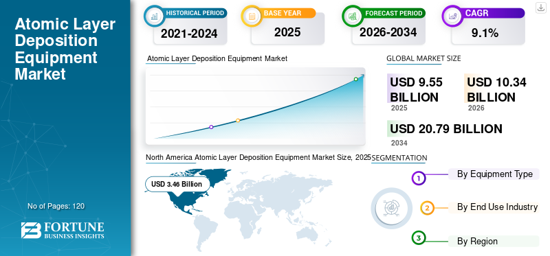
The global atomic layer deposition equipment market size was valued at USD 9.55 billion in 2025. The market is projected to grow from USD 10.34 billion in 2026 to USD 20.79 billion by 2034, exhibiting a CAGR of 9.1% during the forecast period. North America dominated the global atomic layer deposition equipment market with a market share of 36.23% in 2025.
Atomic Layer Deposition (ALD) equipment is specialized manufacturing machinery used to deposit ultra-thin, uniform, and highly controlled material layers onto a substrate (such as silicon wafers) one atomic layer at a time. It enables formation of thin films through sequential, self-limiting chemical reactions, ensuring precise thickness control. The market is witnessing strong growth owing to factors such as device scaling, 3D architectures, advanced packaging growth, shift toward selective deposition, and productivity enhancement. The increasing demand for SiC/GaN power devices, industrial, and consumer durable products will further boost market growth.
- For instance, in February 2025, Lam Research Corporation introduced ALTUS Halo, a next-gen ALD system for molybdenum deposition. The equipment specializes in high-precision and low resistance for advanced logic and memory scaling.
ASM International N.V., Tokyo Electron Limited, Applied Materials, Inc., and Lam Research Corporation are among the key players holding a significant market share. Technology leadership, wide product offerings, high capital investments, and a strong customer portfolio are responsible for the dominance of key players in the market.
Download Free sample to learn more about this report.
ATOMIC LAYER DEPOSITION EQUIPMENT MARKET KEY TAKEAWAYS
- 2025 Market Size: USD 9.55 billion
- 2026 Market Size: USD 10.34 billion
- 2034 Forecast Market Size: USD 20.79 billion
- CAGR: 9.1% from 2026–2034
- North America dominated the atomic layer deposition equipment market with a 36.23% share in 2025.
- Single-wafer ALD systems held the largest share due to their superior process control and semiconductor manufacturing capabilities.
- Semiconductor manufacturing accounted for nearly 50% of the global market in 2025.
North America
North America generated USD 3.46 billion in 2025, supported by strong semiconductor and advanced electronics demand.
Europe
Europe witnessed steady growth due to rising demand for automotive electronics, power devices, and renewable energy applications
Asia Pacific
Asia Pacific recorded USD 3.21 billion in 2025 and remained the fastest-growing regional market.
U.S.
The U.S. atomic layer deposition equipment market is projected to reach USD 3.18 billion in 2026.
Japan
Japan’s atomic layer deposition equipment market is expected to reach USD 0.71 billion in 2026, accounting for 6.9% of global revenue.
Read More
ATOMIC LAYER DEPOSITION EQUIPMENT MARKET TRENDS
Integration of Advanced Technology to be a New Market Trend
Semiconductor fabrication facilities and industrial manufacturers are constantly prioritizing minimal environmental impact. Additionally, these facilities demand energy-efficient and durable equipment to meet stringent ESG and regulatory policies. In order to meet customer requirements, ALD manufacturers are improving chemical utilization efficiency and reducing energy consumption per wafer for the equipment. Integrating technology such as advanced process control, AI-driven diagnostics, and real-time monitoring to further bolster the atomic layer deposition equipment market growth.
- For example, in March 2025, ASM International introduced upgrades to its Pulsar ALD platform focused on improving precursor efficiency and reducing chemical waste, helping advanced fabs lower cost-of-ownership while meeting sustainability targets.
Download Free sample to learn more about this report.
MARKET DYNAMICS
MARKET DRIVERS
Rising Logic and Memory Demand Increases Process Complexity, Driving ALD Equipment Adoption
The high demand for logic and memory will primarily drive the ALD equipment market growth. Data centers, automotive, and consumer electronics, IoT applications, are other factors fueling product demand. EVs, ADAS systems, 5G technology, consumer and industrial electronics, and healthcare electronics require ALD equipment due to their reliability and thermal performance. As these end-use industries expand, they increase both wafer volumes and process complexity, resulting in a higher number of ALD steps per wafer and sustained demand for ALD equipment.
- For instance, in November 2025, Beneq introduced its Transmute high throughput ALD platform, designed for high volume manufacturing of power, RF, and µLED devices, enabling semiconductor industry manufacturers to scale ALD processes for industrial production while improving throughput and process stability.
MARKET RESTRAINTS
High Capital Investment and Lower Throughput to Limit Market Expansion
Atomic layer deposition equipment involves complex system architecture and advanced process control, resulting in significantly higher upfront investment compared to conventional deposition tools. Additionally, the inherently slower deposition rates of ALD can reduce throughput and increase the overall cost of ownership. In high-volume manufacturing environments, the substantial initial cost of ALD equipment further constrains its adoption, limiting its use to critical and high-value applications.
MARKET OPPORTUNITIES
Rising Adoption of ALD in Non-Semiconductor Applications Drive Growth Prospects
Medical devices, sensors, MEMS, and other applications, are gaining huge traction for the equipment owing to their biocompatible coating and precise thickness control. Non-semiconductor applications largely depend on ALD systems for their uniform and thin deposits on complex surfaces. ALD is used in OLED encapsulation, energy storage, batteries, and other devices, which create opportunities for increased revenue. Furthermore, the equipment is also made suitable for temperature-sensitive substrates, driving the demand for low-temperature ALD equipment.
- For instance, in January 2024, Picosun Group launched a new PicoMeDICAL product line of ALD equipment, service, and support focusing on the healthcare industry.
MARKET CHALLENGES
High Process Complexity and Integration Requirements Challenge Market Growth
Process complexity and integration challenges remain a major hurdle in the atomic layer deposition equipment market, as ALD requires extremely precise control over process parameters such as temperature, pressure, pulse timing, and precursor chemistry. Even minor deviations can impact film thickness, uniformity, and device performance, increasing the risk of yield loss. Integrating ALD tools into existing semiconductor fabrication lines also demands extensive process development, tool qualification, and compatibility with upstream and downstream steps. This often lengthens production ramp-up times and increases engineering costs. Additionally, ALD systems require highly skilled operators and process engineers, creating operational challenges for fabs, particularly in regions facing talent shortages.
Segmentation Analysis
By Equipment Type
Superior Process Control and Advanced Node Compatibility Driving Dominance of Single-Wafer ALD Systems
Based on equipment type, the market is divided into single-wafer ALD systems, batch ALD systems, roll-to-roll ALD systems, and spatial ALD systems.
Single-wafer ALD systems to dominate the global atomic layer deposition market share. Single-wafer ALD systems offer superior process control, flexibility, and suitability for advanced semiconductor manufacturing. These systems enable precise, wafer-level control over film thickness, uniformity, and composition, which is critical for leading-edge logic and memory nodes. Single-wafer tools are widely adopted in High-Volume Manufacturing (HVM) as they offer better integration with complex process flows and faster recipe optimization compared to batch systems. Single-wafer ALD systems support a broader range of materials and processes, including selective ALD and metal ALD, making them dominant across the global market.
- For instance, in September 2025, Forge Nano announced to launch its TEPHRA One single-wafer thermal ALD platform designed for 200 mm wafer semiconductor fabs.
Spatial ALD systems are projected to witness a growth rate 9.8% owing to their significant advantages in throughput and scalability for large-area and high-volume applications. The rise of next-generation displays, solar modules, and others, enhance demand for spatial ALD systems.
To know how our report can help streamline your business, Speak to Analyst
By End Use Industry
Device Miniaturization and 3D Architectures Drive Increased Adoption of ALD Equipment in High-Volume Semiconductor Manufacturing
Based on end use industry, the market is segmented into semiconductor manufacturing, electronics manufacturing, energy & power, healthcare, and industrial manufacturing.
Semiconductor manufacturing segment is expected to dominate the global atomic layer deposition equipment market, accounting for half of the global market. ALD equipment plays a critical role in advanced chip fabrication and device scaling. As semiconductor devices continue to shrink and transition to complex 3D architectures such as FinFETs, Gate-All-Around (GAA) transistors, and 3D NAND ALD has become indispensable for depositing ultra-thin, conformal films with atomic-level precision. Rising demand from end markets such as AI, data centers, automotive electronics, and consumer devices is driving high-volume wafer production, further increasing ALD tool installations in semiconductor fabs.
The energy & power segment is expected to witness the highest growth rate of about 9.7% for Atomic Layer Deposition (ALD) equipment due to the rapid expansion of clean energy technologies and power electronics. ALD is increasingly used in the fabrication of wide-bandgap semiconductors such as Silicon Carbide (SiC) and Gallium Nitride (GaN), which are critical for electric vehicles, renewable energy systems, fast chargers, and smart grids. As global investments in electrification and renewable energy accelerate, the adoption of ALD equipment in the energy and power sector is expected to grow at a faster pace than in other end use industries.
Atomic Layer Deposition Equipment Market Regional Outlook
By geography, the market is categorized into Europe, North America, Asia Pacific, South America, and the Middle East & Africa.
North America
North America Atomic Layer Deposition Equipment Market Size, 2025 (USD Billion)
To get more information on the regional analysis of this market, Download Free sample
The North America atomic layer deposition equipment market accounts for over USD 3.46 billion revenue generated in 2025. The market is driven by strong demand from the semiconductor and advanced electronics industries. The region benefits from the presence of leading chip manufacturers, robust R&D infrastructure, and early adoption of next-generation fabrication technologies. Increasing investments in power electronics, MEMS, and medical devices further support market expansion. Additionally, stringent quality and performance standards encourage the adoption of precision deposition tools such as ALD.
U.S. Atomic Layer Deposition Equipment Market
The U.S. dominates the North American market and is anticipated to hit a revenue of about USD 3.18 billion in 2026, primarily driven by strong outbound atomic layer deposition equipment flows and high transaction volumes. Advanced banking infrastructure and widespread adoption of digital and mobile atomic layer deposition equipment platforms further support market leadership. Additionally, the presence of major banks, fintech companies, and atomic layer deposition equipment providers enhances service accessibility, speed, and transparency.
Europe
Europe’s market growth is supported by rising demand for advanced materials in automotive electronics, power devices, and renewable energy applications. The region’s focus on sustainable manufacturing and compliance with strict environmental regulations is encouraging the use of energy-efficient and low-waste deposition technologies. Growth in research institutes and collaborative semiconductor programs across Germany, France, and the Netherlands also contributes to steady market development.
U.K. Atomic Layer Deposition Equipment Market
The U.K. market in 2026 is estimated at around USD 0.37 billion, representing roughly 3.6% of global revenues.
Germany Atomic Layer Deposition Equipment Market
Germany’s atomic layer deposition equipment market is projected to reach approximately USD 0.63 billion in 2026, equivalent to around 6.1% of global sales.
Asia Pacific
Asia Pacific remains the fastest growing market and generated revenue of USD 3.21 billion in 2025. The region’s dominance is owing to the strong presence of major semiconductor foundries and electronics manufacturing hubs in China, Taiwan, South Korea, and Japan. Rapid expansion of consumer electronics, memory chips, and advanced logic devices continues to drive high-volume adoption of ALD tools. Significant government investments in domestic semiconductor production and the growing electric vehicle and battery industries further reinforce the region’s strong growth.
China Atomic Layer Deposition Equipment Market
China’s market is projected to sustain dominance in Asia Pacific, with 2026 revenues estimated at around USD 1.20 billion. This roughly represents 11.6% of global sales.
Japan Atomic Layer Deposition Equipment Market
In 2026, Japan’s atomic layer deposition equipment market will reach USD 0.71 billion, capturing approximately 6.9% share of the global market.
ASEAN Atomic Layer Deposition Equipment Market
The ASEAN atomic layer deposition equipment market in 2026 is estimated at around USD 0.41 billion, accounting for roughly 4.0% of global atomic layer deposition equipment revenues.
Middle East & Africa
The Middle East & Africa market is driven by increasing industrialization and government-led initiatives to diversify economies beyond oil and gas. Rising investments in advanced manufacturing, renewable energy, and research infrastructure are creating new opportunities for ALD adoption.
GCC Atomic Layer Deposition Equipment Market
The GCC market is projected to reach around USD 0.12 billion in 2026, representing roughly 1.1% of the global market.
South America
Brazil and Argentina are increasing investments in semiconductor research, renewable energy technologies, and advanced coatings. Although large-scale semiconductor fabrication is limited, the growing demand for precision coating solutions in industrial and medical applications is contributing to steady market progress.
Brazil Atomic Layer Deposition Equipment Market
The Brazil market is projected to reach around USD 0.21 billion in 2026, representing roughly 2.1% of the global market.
COMPETITIVE LANDSCAPE
Key Industry Players
Industry Giants are Focused on Delivering Precise and Energy Efficient Equipment to Scale Market Share
The Atomic Layer Deposition (ALD) equipment market is moderately consolidated, characterized by the presence of a limited number of global players offering highly specialized and integrated deposition systems. Key market participants such as Applied Materials, ASM International, Tokyo Electron, Picosun Group, and Beneq are focusing on continuous technological innovation to maintain competitiveness, with strong emphasis on process precision, scalability, and energy efficiency. These companies are investing in advanced process control, AI-enabled diagnostics, and automation to address the evolving requirements of semiconductor fabrication, energy storage, and medical device manufacturing.
Established players are also strengthening their market positions by expanding service portfolios and regional footprints through strategic partnerships with foundries, research institutes, and industrial manufacturers. Enhanced after-sales services, remote monitoring, and process optimization support are being prioritized to reduce tool downtime and improve customer productivity. Additionally, selective acquisitions, capacity expansions, and collaborations are being leveraged to balance a strong installed base with innovation-led growth, enabling companies to address both high-volume manufacturing and emerging application segments.
- For instance, Kalpana Systems, a Dutch Manufacturing company, in November 2024, unveiled its Roll-to-Roll ALD Tools for batteries, packaging, and solar.
LIST OF KEY ATOMIC LAYER DEPOSITION EQUIPMENT COMPANIES PROFILED
- ASM International N.V. (U.S.)
- Tokyo Electron Limited (Japan)
- Applied Materials, Inc. (U.S.)
- Lam Research Corporation (U.S.)
- Veeco Instruments Inc. (U.S.)
- Beneq Oy (Finland)
- Picosun Group (Finland)
- Oxford Instruments plc (U.K.)
- Piotech Inc. (China)
- CVD Equipment Corporation (U.S.)
KEY INDUSTRY DEVELOPMENTS
- September 2025: Forge Nano announced it will showcase a new commercial 200 mm single-module ALD tool, TEPHRA One, at SEMICON Taiwan, tailored for oxide, nitride, and nanolaminate coatings with fast deposition and high precursor efficiency.
- February 2025: Lam Research deployed its new ALD equipment ALTUS® Halo for advanced 3D NAND mass production by global memory corporations, signaling the first major industry roll-out of the technology beyond development.
- January 2025: Forge Nano began on-site demonstrations of its TEPHRA™ cluster tool to partners and customers, reinforcing its role in accelerating ALD deployment at commercial scale.
- November 2024: Beneq sold a new generation ALD machine to 2D Generation to accelerate development of its advanced semiconductor technologies, including graphene-based interconnects, supporting broader innovation in chip fabrication.
- November 2024: Adisyn Ltd. announced its investment in an ALD machine from Beneq to support graphene-coated interconnects, marking a strategic technology collaboration aimed at boosting performance in defense, data center, and cybersecurity semiconductor markets.
REPORT COVERAGE
Request for Customization to gain extensive market insights.
Report Scope & Segmentation
|
ATTRIBUTE |
DETAILS |
|
Study Period |
2021-2034 |
|
Base Year |
2025 |
|
Estimated Year |
2026 |
|
Forecast Period |
2026-2034 |
|
Historical Period |
2021-2024 |
|
Growth Rate |
CAGR of 9.1% from 2026-2034 |
|
Unit |
Value (USD Billion) |
|
Segmentation |
By Equipment Type, End Use Industry, and Region |
|
By Equipment Type |
· Single-Wafer ALD Systems · Batch ALD Systems · Roll-to-Roll ALD Systems · Spatial ALD Systems |
|
By End Use Industry |
· Semiconductor Manufacturing · Electronics Manufacturing · Energy & Power · Healthcare · Industrial Manufacturing |
|
By Region |
· North America (By Equipment Type, By End Use Industry, and Country) o U.S. (By Equipment Type) o Canada (By Equipment Type) o Mexico (By Equipment Type) · Europe (By Equipment Type, By End Use Industry, and Country/Sub-region) o Germany (By Equipment Type) o U.K. (By Equipment Type) o France (By Equipment Type) o Spain (By Equipment Type) o Italy (By Equipment Type) o BENELUX (By Equipment Type) o Nordics (By Equipment Type) o Russia (By Equipment Type) o Rest of Europe · Asia Pacific (By Equipment Type, By End Use Industry, and Country/Sub-region) o China (By Equipment Type) o Japan (By Equipment Type) o India (By Equipment Type) o South Korea (By Equipment Type) o ASEAN (By Equipment Type) o Oceania (By Equipment Type) o Rest of Asia Pacific · South America (By Equipment Type, By End Use Industry, and Country/Sub-region) o Brazil (By Equipment Type) o Argentina (By Equipment Type) o Rest of South America · Middle East & Africa (By Equipment Type, By End Use Industry, and Country/Sub-region) o GCC Countries (By Equipment Type) o South Africa (By Equipment Type) o North Africa (By Equipment Type) o Israel (By Equipment Type) o Rest of Middle East & Africa |
Frequently Asked Questions
According to Fortune Business Insights, the global market value stood at USD 9.55 billion in 2025 and is projected to reach USD 20.79 billion by 2034.
In 2025, the market value stood at USD 3.46 billion.
The market is expected to exhibit a CAGR of 9.1% during the forecast period of 2026-2034.
By end use industry, the semiconductor manufacturing segment is expected to dominate the market.
Increasing demand for logic and memory increases process complexity, driving ALD equipment adoption.
Applied Materials, ASM International, Tokyo Electron, Picosun Group, and Beneq are the major players in the global market.
North America held the largest share of the market in 2025.


- 2021-2034
- 2025
- 2021-2024
- 120
Get 30-60 hrs Free Customization
Expand Regional and Country Coverage, Segments Analysis, Company Profiles, Competitive Benchmarking, and End-user Insights.
Related Reports
-
US +1 833 909 2966 ( Toll Free )
-
Get In Touch With Us