 Download Free Sample



Get a Quote
Receive a tailored pricing based on your needs.
- Choose license type
- Multiple user options
- Custom scope & coverage
- Fast turnaround
"Electrifying your pathway to success through in-depth market research"
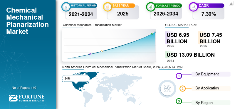
The chemical mechanical planarization market size was valued at USD 13.09 Billion in 2025. The market is projected to grow from USD 7.45 Billion in 2026 to USD 13.09 Billion by 2034, exhibiting a CAGR of 7.30% during the forecast period.

The chemical mechanical planarization market is a critical segment of the semiconductor manufacturing ecosystem, supporting the production of advanced integrated circuits, memory devices, power semiconductors, and emerging electronic components. Chemical Mechanical Planarization (CMP) combines chemical slurry action and mechanical polishing to achieve ultra-flat wafer surfaces required for multilayer semiconductor fabrication. The increasing complexity of chip architectures, growing adoption of artificial intelligence processors, advanced packaging technologies, and high-density memory devices are accelerating CMP implementation across fabrication facilities. Chemical mechanical planarization market analysis indicates that CMP equipment and consumables remain indispensable for achieving precision, yield enhancement, and defect reduction in modern wafer manufacturing environments.
Download Free sample to learn more about this report.
The United States represents a major center for chemical mechanical planarization technology adoption due to strong semiconductor manufacturing investments, advanced research programs, and domestic fabrication expansion initiatives. CMP demand is closely linked to the development of advanced logic chips, defense electronics, automotive semiconductors, and artificial intelligence processors. New wafer fabrication projects continue to increase the installation of CMP equipment and associated consumables. The USA chemical mechanical planarization market outlook remains supported by ongoing technological innovation, increased production of high-performance computing chips, and expansion of advanced packaging facilities. Semiconductor process optimization and defect reduction requirements further strengthen CMP deployment across fabrication plants.
 Global Market Size & Forecast
 Market Share
 Key Regional Highlights
Asia-Pacific
Asia-Pacific led the market with a 46% share, supported by strong semiconductor manufacturing activity and expanding wafer production.
North America
North America accounted for 24% of the market, driven by advanced semiconductor technologies and investments in chip manufacturing.
Europe
Europe held a 20% share, supported by established semiconductor capabilities and growing demand for advanced electronic components.
U.S
The U.S. remains a key market, supported by advanced semiconductor manufacturing and increasing investments in domestic chip production.
Japan
Japan accounted for approximately 21% of the Asia-Pacific market, supported by its established semiconductor industry and advanced manufacturing capabilities.
Read More

One of the most significant chemical mechanical planarization market trends is the transition toward sub-5 nanometer semiconductor nodes. Advanced chip designs require multiple planarization steps to ensure layer uniformity and maintain manufacturing precision. Manufacturers are increasingly deploying highly specialized slurries and polishing pads designed for copper, tungsten, dielectric, and silicon carbide applications. The emergence of three-dimensional NAND memory and heterogeneous integration technologies is also increasing CMP process intensity across fabrication workflows.
Download Free sample to learn more about this report.
Another important trend involves automation and process intelligence. Semiconductor manufacturers are integrating advanced metrology systems with CMP equipment to monitor polishing performance in real time. Artificial intelligence-assisted process control is helping fabs improve wafer yield and reduce defects. Growth in electric vehicles, cloud computing infrastructure, data centers, and high-performance processors is generating additional demand for advanced semiconductor devices, which directly supports chemical mechanical planarization market growth. Furthermore, compound semiconductor applications involving gallium nitride and silicon carbide are creating new opportunities for CMP solution providers.
Growing Demand for Advanced Semiconductor Devices and Wafer Fabrication Expansion
The primary driver of the chemical mechanical planarization market is the continuous increase in semiconductor manufacturing complexity. Advanced logic chips, AI accelerators, memory devices, and high-performance computing processors require extremely flat wafer surfaces for reliable functionality. CMP enables manufacturers to achieve the necessary precision during multiple fabrication stages. Semiconductor foundries are expanding production capacity to support demand from consumer electronics, telecommunications infrastructure, automotive electronics, and industrial automation systems.
The increasing deployment of 5G networks, cloud computing platforms, and artificial intelligence applications is creating additional semiconductor demand. Modern chip architectures involve a greater number of layers, making planarization increasingly essential. CMP technology also supports advanced packaging methods, which are becoming crucial for next-generation semiconductor performance. As global fabrication facilities adopt more sophisticated manufacturing processes, demand for CMP equipment, slurries, pads, and process optimization solutions continues to expand.
High Equipment Complexity and Operational Requirements
Despite strong adoption, the chemical mechanical planarization market faces restraints associated with equipment complexity and process sensitivity. CMP operations require strict control of pressure, slurry chemistry, pad condition, and polishing duration. Even minor variations can affect wafer quality and production yields. Semiconductor manufacturers must invest heavily in process development and ongoing optimization activities.
The requirement for specialized consumables also contributes to operational challenges. Polishing pads and slurries must be continuously monitored and replaced according to precise specifications. Advanced node manufacturing demands increasingly sophisticated consumable formulations, creating additional qualification requirements. Furthermore, the need for highly skilled personnel capable of managing CMP operations can limit rapid deployment in emerging semiconductor manufacturing regions. These factors increase operational complexity and may delay implementation timelines for certain facilities.
Expansion of Compound Semiconductors and Advanced Packaging Technologies
The growth of compound semiconductor manufacturing presents substantial opportunities within the chemical mechanical planarization market. Silicon carbide and gallium nitride devices are becoming increasingly important for electric vehicles, renewable energy systems, industrial power electronics, and telecommunications infrastructure. These materials require specialized planarization solutions, creating new market opportunities for equipment suppliers and consumable manufacturers.
Advanced packaging technologies represent another major growth avenue. Chiplet architectures, heterogeneous integration, and three-dimensional packaging methods require precise surface preparation to ensure optimal performance. Semiconductor manufacturers are investing in innovative packaging approaches to improve computing efficiency and reduce power consumption. CMP plays a vital role in enabling these developments by ensuring surface uniformity throughout the manufacturing process. As advanced packaging adoption accelerates, CMP demand is expected to expand across multiple semiconductor segments.
Defect Control and Process Uniformity Requirements
Maintaining defect-free wafer surfaces remains one of the most significant challenges in the chemical mechanical planarization industry analysis. Semiconductor manufacturers must achieve extremely high levels of uniformity while minimizing scratches, contamination, dishing, erosion, and other surface defects. As semiconductor nodes continue to shrink, acceptable process tolerances become increasingly narrow.
Manufacturers also face challenges related to slurry particle control, pad conditioning consistency, and equipment calibration. Variations across large wafer diameters can affect final device performance and manufacturing yield. The transition toward advanced semiconductor structures introduces additional process complexity, requiring continuous innovation in CMP technologies. Meeting increasingly stringent performance standards while controlling operational costs remains a key challenge for industry participants seeking long-term competitiveness.
CMP Equipment accounts for approximately 59% of the chemical mechanical planarization market share. This segment includes polishing systems, platen assemblies, wafer carriers, endpoint detection systems, and integrated cleaning modules. Semiconductor manufacturers depend on advanced CMP equipment to achieve precision planarization during multiple wafer processing stages. Equipment demand is particularly strong among foundries and integrated device manufacturers producing advanced logic and memory devices.
The growing number of CMP process steps required for advanced semiconductor nodes continues to support equipment adoption. Modern CMP platforms offer enhanced automation, process monitoring, and defect control capabilities. Demand is also increasing in facilities focused on advanced packaging and compound semiconductor production. Chemical mechanical planarization market research report findings indicate that equipment suppliers are investing heavily in productivity improvements, throughput optimization, and process integration solutions to address evolving semiconductor manufacturing requirements.
CMP Consumables represent approximately 41% of the chemical mechanical planarization market size. This segment includes polishing slurries, polishing pads, conditioning disks, cleaning chemicals, and related process materials. Consumables are essential for maintaining polishing efficiency and wafer quality throughout production operations. Continuous wafer processing generates recurring demand, making consumables a strategically important market segment.
Advanced semiconductor manufacturing increasingly requires customized slurry formulations designed for specific materials such as copper, tungsten, dielectric layers, and silicon carbide. Manufacturers are focusing on consumables that improve defect reduction, polishing selectivity, and process stability. The expansion of advanced packaging technologies and compound semiconductor production is creating additional opportunities for consumable innovation. As semiconductor manufacturing volumes increase globally, consumable demand remains closely linked to wafer production growth.
Integrated Circuits account for approximately 67% of the chemical mechanical planarization market share, making them the dominant application segment. CMP is fundamental to integrated circuit manufacturing because modern chips contain multiple layers requiring precise planarization. Smartphones, computers, networking equipment, cloud infrastructure, and artificial intelligence systems all rely on advanced integrated circuits manufactured using CMP processes.
Increasing transistor density and complex chip architectures continue to elevate CMP requirements within integrated circuit production. Semiconductor manufacturers require superior surface flatness to maintain electrical performance and manufacturing yields. Advanced logic devices and memory chips often undergo multiple CMP steps throughout production. The continued expansion of digital transformation initiatives, artificial intelligence deployment, and high-performance computing infrastructure supports long-term growth within this application segment.
Automotive applications account for approximately 33% of the chemical mechanical planarization market. Vehicle electrification, autonomous driving systems, advanced driver assistance technologies, and connected mobility solutions are increasing semiconductor content within modern vehicles. Automotive semiconductor manufacturers utilize CMP technology to produce sensors, microcontrollers, power devices, and communication components.
The transition toward electric vehicles is creating strong demand for power semiconductors based on silicon carbide and other advanced materials. These applications require specialized planarization techniques capable of meeting stringent reliability requirements. Automotive manufacturers also require highly durable semiconductor devices capable of operating under demanding environmental conditions. As vehicle electronics become increasingly sophisticated, CMP adoption within automotive semiconductor manufacturing is expected to expand significantly.
To know how our report can help streamline your business, Speak to Analyst
North America Chemical Mechanical Planarization Market Share, 2026 (%)
To get more information on the regional analysis of this market, Download Free sample
North America remains a strategically important region due to semiconductor manufacturing expansion, advanced research capabilities, and investments in domestic chip production. The region benefits from strong demand for high-performance computing, artificial intelligence processors, defense electronics, and advanced communication systems. CMP equipment installation activity continues to increase as fabrication facilities expand production capabilities. Regional manufacturers focus on process innovation, advanced packaging, and next-generation semiconductor technologies. The chemical mechanical planarization market forecast for North America remains supported by ongoing investments in fabrication infrastructure and semiconductor supply chain development.
Europe maintains a significant position within the chemical mechanical planarization market through its strengths in automotive electronics, industrial automation, power semiconductor manufacturing, and research-driven innovation. Regional semiconductor producers increasingly focus on energy-efficient devices, electric vehicle technologies, and industrial digitalization. Investments in semiconductor manufacturing capacity and advanced packaging capabilities support regional CMP demand. Process optimization, sustainability initiatives, and manufacturing quality standards continue to drive adoption of advanced planarization solutions across European facilities.
Germany accounts for approximately 32% of the European chemical mechanical planarization market. The country serves as a major center for automotive semiconductor production, industrial automation technologies, and advanced manufacturing systems. Demand for CMP solutions is supported by increasing semiconductor content in electric vehicles, factory automation platforms, and intelligent industrial equipment.
German semiconductor manufacturers emphasize production precision, process reliability, and technological innovation. The expansion of power semiconductor manufacturing and silicon carbide device production is creating new opportunities for CMP technology providers. Research institutions and industrial collaborations continue to support the development of advanced semiconductor manufacturing techniques. As automotive electrification accelerates, Germany remains a key contributor to regional CMP demand.
The United Kingdom represents approximately 18% of the European chemical mechanical planarization market. The country benefits from strong semiconductor research capabilities, specialized microelectronics expertise, and growing interest in advanced technology applications. CMP demand is supported by research-driven semiconductor development, aerospace electronics, defense technologies, and communication infrastructure projects.
The UK semiconductor ecosystem increasingly focuses on innovative chip design, photonics, and specialized manufacturing processes. Collaboration between industry and research organizations supports ongoing technological advancement. Demand for advanced semiconductor devices used in telecommunications, artificial intelligence, and defense systems contributes to CMP market expansion. Continued investment in high-value semiconductor applications strengthens the country's role within the regional market.
Asia-Pacific dominates the global chemical mechanical planarization market due to its concentration of semiconductor foundries, memory manufacturers, and electronics production facilities. Regional demand is driven by large-scale wafer fabrication operations, advanced packaging investments, and strong consumer electronics manufacturing activity. Major semiconductor manufacturing hubs continue expanding production capacity to meet global demand. Advanced logic chips, memory devices, and power semiconductors collectively support extensive CMP utilization.
Japan accounts for approximately 21% of the Asia-Pacific chemical mechanical planarization market. The country plays a critical role in semiconductor materials, manufacturing equipment, and process technology development. Japanese companies maintain strong positions in CMP consumables, precision equipment, and specialty materials required for advanced wafer processing.
Demand for CMP solutions is supported by semiconductor manufacturing, automotive electronics, industrial automation systems, and advanced sensor technologies. Japanese manufacturers emphasize production quality, process consistency, and technological innovation. Continuous investments in semiconductor materials and equipment development help sustain market growth. The country's expertise in precision manufacturing supports long-term demand for advanced planarization technologies.
China represents approximately 38% of the Asia-Pacific chemical mechanical planarization market. The country continues expanding semiconductor manufacturing capacity through investments in fabrication facilities, equipment procurement, and domestic supply chain development. Demand for CMP equipment and consumables is increasing across logic chip, memory device, and power semiconductor production.
The rapid growth of consumer electronics, electric vehicles, telecommunications infrastructure, and industrial automation supports semiconductor demand throughout the country. Domestic semiconductor manufacturers are investing in advanced process technologies to improve competitiveness. As fabrication capacity expands, CMP adoption continues to increase across multiple semiconductor applications, strengthening China's position within the regional market.
The Rest of World region includes the Middle East, Africa, and Latin America. Although semiconductor manufacturing activity remains smaller compared with major production hubs, growing investments in electronics assembly, industrial modernization, telecommunications infrastructure, and technology development support gradual CMP market expansion. Regional governments increasingly recognize the strategic importance of semiconductor capabilities and advanced manufacturing technologies.
Demand for semiconductor devices continues to rise due to digital transformation initiatives, industrial automation projects, and expanding communication networks. Emerging opportunities related to electric mobility, renewable energy systems, and industrial electronics are expected to support future CMP adoption. Strategic partnerships and technology transfer initiatives are also contributing to regional market development.
Investment activity within the chemical mechanical planarization market is increasing due to ongoing semiconductor fabrication expansion worldwide. Manufacturers are allocating capital toward new CMP equipment installations, consumable production facilities, and process development initiatives. Advanced packaging technologies, artificial intelligence processors, and high-bandwidth memory applications are creating attractive investment opportunities throughout the semiconductor value chain.
Investors are particularly interested in companies developing next-generation slurries, advanced polishing pads, endpoint detection systems, and automation software. Growth opportunities are also emerging in silicon carbide and gallium nitride semiconductor production. Strategic partnerships between semiconductor manufacturers, material suppliers, and equipment providers continue to support innovation. Chemical mechanical planarization market opportunities remain strong as chip complexity increases and semiconductor production volumes expand across multiple end-use industries.
Innovation remains a central focus of the chemical mechanical planarization market. Manufacturers are introducing advanced polishing systems equipped with artificial intelligence-driven process controls, predictive maintenance capabilities, and integrated metrology solutions. These technologies improve wafer uniformity, reduce defects, and enhance manufacturing efficiency.
New consumable formulations are also being developed to support advanced semiconductor materials and packaging architectures. Slurries designed for copper, tungsten, dielectric, and silicon carbide applications offer improved selectivity and polishing performance. Pad technologies continue evolving to provide better consistency and reduced defect generation. Equipment suppliers are focusing on throughput enhancement, automation integration, and energy efficiency improvements. These innovations support the production requirements of advanced logic devices, memory chips, and power semiconductors.
The chemical mechanical planarization market report provides detailed coverage of market structure, technology developments, competitive landscape, application analysis, and regional performance. The report evaluates CMP equipment and consumable segments while examining their role within semiconductor manufacturing operations. Key market drivers, restraints, opportunities, and challenges are assessed to provide a comprehensive understanding of industry dynamics.
Request for Customization to gain extensive market insights.
The report also analyzes integrated circuit and automotive applications, highlighting demand patterns and technological developments influencing market evolution. Regional assessments cover North America, Europe, Asia-Pacific, and Rest of World markets, while country-level evaluations examine major semiconductor manufacturing centers. Competitive analysis includes leading equipment providers, consumable manufacturers, and technology innovators. Chemical Mechanical Planarization Industry Report findings support strategic planning, investment evaluation, and business development activities for stakeholders across the semiconductor ecosystem.
Fortune Business Insights says that the global market value stood at USD 6.95 billion in 2025 and is projected to reach USD 13.09 billion by 2034.
The market is expected to exhibit a CAGR of 7.30% during the forecast period of 2026-2034.
Integrated Circuits was the leading application segment, accounting for approximately 67% of the market, driven by the increasing need for precise planarization in multilayer chip manufacturing.
Key players include Applied Materials Inc., Entegris Inc., Ebara Corporation, Lapmaster Wolters GmbH, DuPont de Nemours Inc., and Fujimi Incorporated.
Major trends include the shift toward sub-5 nanometer semiconductor nodes and greater adoption of automation, advanced metrology, and AI-assisted process control. Asia-Pacific dominated with a 46% market share.


(Offer valid till 15th Nov 2026)
Get 30-60 hrs Free Customization
Expand Regional and Country Coverage, Segments Analysis, Company Profiles, Competitive Benchmarking, and End-user Insights.




















Get In Touch With Us
US +1 833 909 2966 ( Toll Free )
Receive a tailored pricing based on your needs.
Discuss your questions with our industry experts.
Have questions? Get quick answers before you purchase.

