Wafer Handling Robots Market Size, Share & Industry Analysis, By Type (Vacuum and Atmospheric), By Robot Configuration (Single Arm and Dual Arm), By Application (Front-End Processing, Back-End (Assembly & Packaging), and Inspection & Metrology), and By End User (Integrated Device Manufacturers (IDMs), Foundries, and Outsourced Semiconductor Assembly and Test (OSAT)), and Regional Forecast, 2026 – 2034
Wafer Handling Robots Market Size and Future Outlook
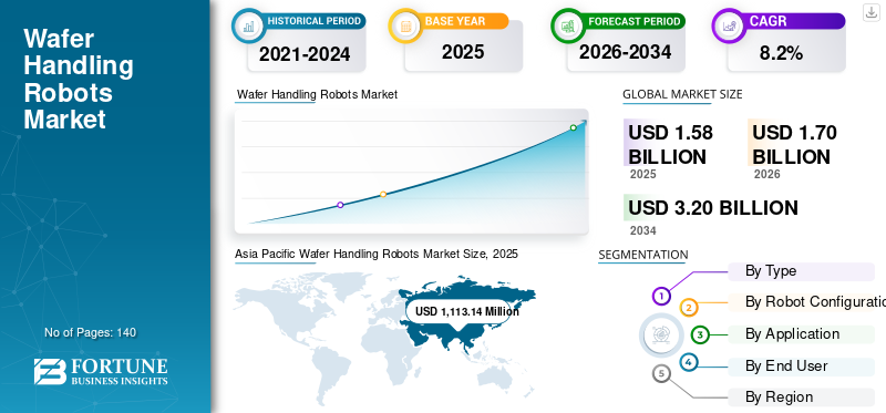
The global wafer handling robots market size was valued at USD 1,588.89 million in 2025. The market is projected to grow from USD 1,707.55 million in 2026 to USD 3,204.78 million by 2034, exhibiting a CAGR of 8.2% during the forecast period. Asia Pacific dominated the wafer handling robots market with a market share of 70.0% in 2025.
Wafer handling robots help semiconductor manufacturers automate critical wafer transfer processes, enabling precise, contamination-free movement of semiconductor wafers across fabrication, inspection, and packaging stages. These systems play a crucial role in the semiconductor manufacturing process by integrating high-precision robotic arms, vacuum end-effectors, advanced motion control, and cleanroom-compatible software to enhance throughput, minimize particle contamination, and improve process reliability in semiconductor fabs. Continuous technology advances in robotics and automation are further supporting the adoption of these solutions, helping manufacturers enhance productivity and maintain high yield levels. The industry is witnessing steady growth as chip manufacturers increase investments in advanced fabrication facilities driven by rising demand for AI, automotive electronics, and high-performance computing. Growing deployment of automated wafer handling solutions across 300mm fabs, advanced node manufacturing, and OSAT facilities is driving demand across Asia Pacific, North America, and Europe, contributing to the overall market size.
- For instance, in February 2026, RORZE Corporation introduced next-generation vacuum wafer handling robots designed for advanced semiconductor nodes, featuring enhanced precision control and optimized cleanroom performance to support high-throughput wafer processing in modern fabrication environments.
Brooks Automation (Azenta Inc.), RORZE Corporation, Hirata Corporation, Kawasaki Heavy Industries Ltd., and DAIHEN Corporation are among the key players holding a significant share of the market. Their competitive positioning is supported by specialized semiconductor robotics expertise, high-precision automation solutions, strong integration capabilities with semiconductor equipment OEMs, and the ability to deliver scalable wafer handling systems tailored for front-end and back-end semiconductor manufacturing applications.
Download Free sample to learn more about this report.
Wafer Handling Robots Market Key Takeaways
- 2025 Market Size: USD 1,588.89 million
- 2026 Market Size: USD 1,707.55 million
- 2034 Forecast Market Size: USD 3,204.78 million
- CAGR: 8.2% from 2026–2034
- Asia Pacific dominated the wafer handling robots market with a 70.0% share in 2025.
- Atmospheric wafer handling robots are projected to expand at a CAGR of 7.0% during the forecast period.
- Inspection & metrology applications are expected to grow at a CAGR of 7.3% over the study period.
Asia Pacific
Asia Pacific remained the leading regional market in 2025, generating revenue of USD 1,113.14 million due to strong semiconductor manufacturing activity.
North America
North America accounted for over USD 247.54 million in market revenue in 2025, supported by rising investments in advanced chip fabrication facilities.
Europe
Europe is witnessing steady market expansion driven by increasing automation adoption in semiconductor production and inspection processes.
U.S.
The U.S. wafer handling robots market is expected to dominate North America with estimated revenue of USD 237.47 million in 2026.
Japan
Japan’s wafer handling robots market is estimated at USD 219.74 million in 2026, accounting for approximately 12.9% of global sales.
Read More
WAFER HANDLING ROBOTS MARKET TRENDS
Increasing Semiconductor Fab Expansion and Advanced Node Manufacturing is Reshaping Market Demand
The demand for such robots is increasingly influenced by the rapid expansion of semiconductor fabrication facilities and the transition toward advanced node manufacturing across global semiconductor supply chains. Chip manufacturers are prioritizing automation of wafer transfer and handling processes to improve throughput, minimize contamination risks, and enhance precision across critical fabrication stages such as lithography, etching, and deposition. These evolving priorities are driving the adoption of high-precision robotic systems integrated with vacuum end-effectors, advanced motion control, and cleanroom-compatible technologies capable of handling delicate wafers in ultra-clean environments. Organizations are expanding automation investments beyond conventional fabs toward advanced 300mm facilities and next-generation semiconductor manufacturing ecosystems, where precision, reliability, and scalability are critical. These developments are influencing market dynamics as semiconductor companies adopt fully automated fabrication environments, real-time process monitoring, and integrated material handling systems to improve yield and operational efficiency. Solution providers are responding by introducing advanced wafer handling robots with enhanced precision, modular configurations, and seamless integration with semiconductor equipment and factory automation systems, enabling improved productivity across complex fabrication environments.
- For instance, in March 2025, Brooks Automation (Azenta Inc.) expanded its semiconductor automation portfolio by introducing advanced vacuum wafer handling systems designed to support high-throughput and contamination-free wafer transfer in next-generation semiconductor fabrication facilities.
MARKET DYNAMICS
MARKET DRIVERS
Rising Semiconductor Demand and Fab Automation to Drive Market Growth
The market is experiencing accelerated growth as semiconductor manufacturers increasingly adopt automation to meet rising demand for advanced chips and improve fabrication efficiency. Companies across IDMs, foundries, and OSAT facilities are prioritizing the automation of wafer transfer processes to enhance throughput, reduce contamination risks, and ensure precision in critical fabrication stages. The expansion of applications such as artificial intelligence, electric vehicles, and high-performance computing is further driving demand for advanced semiconductor manufacturing, increasing the need for reliable and high-speed wafer handling solutions. As fabrication complexity increases with the transition to smaller technology nodes and larger wafer sizes, organizations are investing in high-precision robotic systems integrated with vacuum handling, advanced motion control, and cleanroom-compatible technologies to improve yield and scalability. Solution providers are responding by expanding their portfolios with advanced wafer handling robots that support seamless integration with semiconductor equipment and factory automation systems, enabling manufacturers to optimize production efficiency and maintain consistent performance across high-volume fabrication environments.
- For instance, in 2025, RORZE Corporation expanded its semiconductor robotics portfolio with advanced vacuum wafer handling systems designed to support high-throughput and contamination-free wafer transfer in modern semiconductor fabrication facilities.
Download Free sample to learn more about this report.
MARKET RESTRAINTS
High System Cost and Integration Complexity to Constrain Market Expansion
Unlike conventional industrial automation systems, such robots require significant upfront investment in high-precision robotic hardware, vacuum end-effectors, cleanroom-compatible components, and specialized control software. The deployment of these systems often involves complex integration with semiconductor manufacturing equipment such as lithography, etching, and deposition tools, as well as factory automation and manufacturing execution systems, which can increase implementation timelines and costs. Semiconductor fabrication environments demand extremely high levels of precision and contamination control, requiring customized robotic solutions tailored to specific process requirements, which limits standardization. Additionally, the need for highly skilled personnel to operate, program, and maintain wafer handling robots presents challenges, particularly in regions with limited semiconductor manufacturing expertise. These factors can slow adoption rates, especially for smaller or emerging semiconductor players, and may constrain the rapid expansion of wafer handling automation across new fabrication facilities.
MARKET OPPORTUNITIES
Increasing Demand for Advanced Fab Automation and Modular Semiconductor Equipment Creating New Growth Avenues
An emerging opportunity in the wafer handling robots market growth is the increasing investment in advanced semiconductor fabrication facilities and the adoption of modular automation architectures. Traditionally, such robots were deployed primarily in large-scale, high-volume fabs due to high capital requirements and complex system integration. However, the evolution of semiconductor manufacturing toward modular fab designs, standardized equipment interfaces, and scalable automation frameworks is enabling broader adoption across emerging semiconductor players and new fabrication facilities. Manufacturers are developing compact, high-precision robots with flexible configurations, reduced footprint, and improved integration capabilities to support next-generation fabs and pilot production lines. These systems allow semiconductor companies to scale automation in phases while maintaining strict cleanroom and process requirements. As new entrants and regional semiconductor initiatives continue to expand, demand for flexible, easy-to-integrate wafer handling solutions is expected to increase across both developed and emerging semiconductor markets.
- For instance, in April 2024, Intel announced continued investment in advanced semiconductor manufacturing facilities in the U.S. and Europe. Further, emphasizing increased automation and advanced material handling systems within next-generation fabs to support high-volume and precision wafer processing.
MARKET CHALLENGES
High Precision Requirements and Lack of Standardization in Wafer Handling Interfaces Increasing System Complexity
A critical challenge in the market is the lack of standardization across wafer handling interfaces, end-effectors, and equipment integration requirements within semiconductor manufacturing environments. Different fabrication processes require highly specialized handling mechanisms, including vacuum-based end-effectors, edge-grip systems, and customized wafer transfer configurations to ensure contamination-free and damage-free handling of wafers. This diversity increases system design complexity and often necessitates highly customized engineering for each semiconductor tool and process step. The absence of uniform standards across equipment platforms can lead to longer deployment cycles, higher integration costs, and increased maintenance requirements. Additionally, achieving the required levels of precision, repeatability, and cleanliness in advanced node manufacturing further intensifies system complexity. These challenges can limit scalability and create operational constraints, particularly for semiconductor manufacturers managing multiple process technologies and equipment configurations across fabs.
Segmentation Analysis
By Type
Vacuum Segment Led as It Represents the Core Requirement in Semiconductor Fabrication Environments
By type, the market is segmented into vacuum and atmospheric.
Vacuum held the largest wafer handling robots market share as it represents the primary and most critical requirement across semiconductor fabrication processes. Semiconductor manufacturing environments, particularly front-end wafer processing stages such as lithography, etching, and deposition, require ultra-clean and controlled vacuum conditions to prevent contamination and ensure process precision. As a result, such robots equipped with vacuum-compatible end-effectors and cleanroom-grade components are widely adopted across advanced fabrication facilities. The demand is particularly strong in 300mm fabs and advanced node manufacturing, where maintaining wafer integrity and minimizing particle contamination are essential for achieving high yield and process reliability. As semiconductor manufacturers continue to invest in next-generation fabs and automation systems, there is increasing adoption of high-precision vacuum wafer handling robots integrated with advanced motion control and factory automation systems. These systems enable improved throughput, enhanced process control, and reduced defect rates, making vacuum-based handling the foundational application in semiconductor automation.
- For instance, in April 2025, Taiwan Semiconductor Manufacturing Company (TSMC) announced continued expansion of its advanced semiconductor fabrication capacity, emphasizing increased automation and advanced material handling systems within its next-generation fabs to support high-volume wafer processing.
Atmospheric is an emerging segment and is projected to expand at a CAGR of 7.0% over the study period. The growth of this segment is driven by increasing automation in back-end semiconductor processes, including wafer inspection, testing, and packaging, where ultra-high vacuum conditions are not always required. As OSAT facilities and semiconductor assembly operations expand, organizations are adopting atmospheric wafer handling robots to improve operational efficiency and handle high volumes of wafers in less stringent cleanroom environments.
To know how our report can help streamline your business, Speak to Analyst
By Robot Configuration
Dual Arm Segment Led as It Enhances Throughput and Efficiency in High-Volume Semiconductor Manufacturing
By robot configuration, the market is segmented into single arm and dual arm.
Dual arm held the largest share of the market, driven by its ability to significantly enhance wafer transfer efficiency and throughput in semiconductor fabrication environments. These systems enable simultaneous handling of multiple wafers or parallel processing between load ports and process chambers, reducing cycle time and improving equipment utilization. Dual arm wafer handling robots are widely adopted in high-volume 300mm fabrication facilities and advanced node manufacturing, where speed, precision, and continuous operation are critical. The demand is particularly strong among leading semiconductor manufacturers and foundries, where optimizing wafer movement directly impacts production yield and overall fab productivity.
- For instance, in March 2025, Kawasaki Heavy Industries highlighted its semiconductor robot portfolio, including dual-arm wafer handling robots designed for high-speed wafer transfer and improved productivity in semiconductor manufacturing systems.
Single arm is expected to register steady growth and is projected to expand at a CAGR of 6.8% over the forecast period. The growth of this segment is driven by increasing adoption in specialized and lower-throughput semiconductor processes, including wafer inspection, metrology, and pilot production lines.
By Application
Front-End Processing Segment Led as It Represents the Core of Semiconductor Manufacturing Operations
By application, the market is segmented into front-end processing, back-end (assembly & packaging), and inspection & metrology.
Front-end processing held the largest share of the market, driven by its critical role in semiconductor fabrication processes such as lithography, etching, deposition, and cleaning. These processes require highly precise, contamination-free wafer transfer under controlled cleanroom and vacuum environments, making wafer handling robots an essential component of front-end manufacturing. The demand is particularly strong in advanced node production and 300mm fabs, where high throughput, accuracy, and yield optimization are key operational priorities.
Inspection & metrology is expected to register strong growth and is projected to expand at a CAGR of 7.3% over the study period. The growth of this segment is driven by increasing emphasis on yield improvement, defect detection, and process control in semiconductor manufacturing.
By End User
Integrated Device Manufacturers Segment Led Due to Semiconductor Fabrication and High Production Volumes
Based on end user, the market is segmented into Integrated Device Manufacturers (IDMs), foundries, and Outsourced Semiconductor Assembly and Test (OSAT).
Integrated Device Manufacturers (IDMs) account for the highest share of the market, driven by their extensive semiconductor fabrication operations and high-volume production requirements. IDMs such as Intel, Samsung, and Micron manage end-to-end chip manufacturing, including wafer fabrication, processing, and in some cases packaging, requiring highly automated and precise wafer handling systems. These organizations operate advanced and large-scale fabrication facilities where maintaining throughput, minimizing contamination, and ensuring process consistency are critical.
Foundries are expected to register the highest growth rate in the market, expanding at a CAGR of 9.5% during the study period, driven by the increasing outsourcing of semiconductor manufacturing by fabless companies. Pure-play foundries such as TSMC and GlobalFoundries are rapidly expanding their fabrication capacities to meet growing demand for advanced and specialty chips.
Wafer Handling Robots Market Regional Outlook
By region, the market is categorized into Europe, North America, Asia Pacific, South America, and the Middle East & Africa.
Asia Pacific
Asia Pacific Wafer Handling Robots Market Size, 2025 (USD Million)
To get more information on the regional analysis of this market, Download Free sample
Asia Pacific leads with the largest market share, generating revenue of USD 1,113.14 million in 2025 globally. Within the region, China and Japan are projected to reach approximately USD 329.62 million and USD 219.74 million, respectively by 2026. Asia Pacific remains the fastest-growing market, supported by the region’s dominant position in global semiconductor manufacturing and continuous expansion of fabrication capacity across key economies such as China, Japan, South Korea, Taiwan, and emerging markets such as India. The region’s growth is primarily driven by large-scale semiconductor production, particularly in advanced logic, memory, and mature node manufacturing, where high-volume wafer processing requires precise, contamination-free handling solutions. Countries such as Taiwan and South Korea lead in advanced node manufacturing, while China continues to expand its domestic semiconductor capabilities through significant investments in fabrication infrastructure.
China Wafer Handling Robots Market
China’s market is projected to remain the dominant in the Asia Pacific region, with 2026 revenues estimated at around USD 329.62 million, representing roughly 19.3% of global sales.
Japan Wafer Handling Robots Market
The Japan market in 2026 is estimated at around USD 219.74 million, accounting for roughly 12.9% of the global sales.
India Wafer Handling Robots Market
The India market in 2026 is estimated at around USD 74.04 million, accounting for roughly 4.3% of global sales.
North America
The North America market accounted for over USD 247.54 million in revenue in 2025. The growth is supported by strong semiconductor manufacturing activity, increasing fab investments, and rising adoption of advanced automation technologies across the U.S., Canada, and Mexico. Regional demand is closely linked to the expansion of semiconductor fabrication facilities, government-led initiatives such as the U.S. CHIPS Act, and the growing need for high-precision, contamination-free wafer handling in advanced manufacturing environments. Companies across IDMs, foundries, and semiconductor equipment ecosystems are increasingly investing in automated wafer handling solutions to improve throughput, reduce human intervention, and enhance process reliability.
U.S. Wafer Handling Robots Market
The U.S. is expected to dominate the region with an estimated revenue of about USD 237.47 million in 2026. The growth is driven by the country’s strong semiconductor manufacturing base, increasing investments in advanced fabrication facilities, and rapid adoption of automation across wafer processing operations. Unlike many regions, U.S. semiconductor manufacturers are heavily focused on deploying highly automated fabrication environments to support advanced node production and improve yield efficiency. Leading companies such as Intel, GlobalFoundries, and new entrants including TSMC and Samsung in the U.S. are expanding their fabrication capacities, driving demand for high-performance robots. These systems are widely used across front-end processing, inspection, and material handling operations to ensure precision, minimize contamination, and support high-volume production.
Europe
The European market is supported by a well-established semiconductor and industrial base, strong adoption of advanced automation technologies, and increasing focus on enhancing manufacturing efficiency. The region’s growth is spread across key economies such as Germany, U.K., France, Italy, and Netherlands. The demand for such robots is closely tied to the region’s semiconductor manufacturing capabilities, particularly in automotive, industrial, and power electronics applications, where precision and reliability are critical. Companies across IDMs and semiconductor equipment ecosystems are increasingly adopting automated wafer handling solutions to improve throughput, ensure contamination-free processing, and maintain consistent production quality.
U.K. Wafer Handling Robots Market
The U.K. market in 2026 is estimated at around USD 12.34 million, representing roughly 0.7% of global sales.
Germany Wafer Handling Robots Market
Germany’s market is projected to reach approximately USD 46.12 million in 2026, equivalent to around 2.7% of global sales.
Middle East & Africa
The Middle East & Africa market is driven by increasing investments in semiconductor-related capabilities, advanced manufacturing infrastructure, and growing focus on technology diversification, particularly across Israel, GCC countries, and select North African economies. The demand for such robots is closely linked to the presence of semiconductor fabrication and research activities, as well as emerging initiatives to develop local semiconductor ecosystems. Israel represents the most significant market within the region, supported by the presence of advanced semiconductor fabrication facilities and strong adoption of high-precision automation technologies. GCC countries are witnessing rising investments in high-tech industries, research infrastructure, and electronics manufacturing, contributing to gradual adoption of cleanroom automation and wafer handling solutions.
GCC Wafer Handling Robots Market
The GCC market is projected to reach around USD 12.82 million in 2026, representing roughly 0.8% of the global sales.
South America
The South America market is supported by the region’s limited but gradually developing semiconductor and electronics manufacturing footprint, particularly in Brazil and select emerging economies. Demand for such robots is primarily driven by niche semiconductor activities, government-backed initiatives, and growing interest in strengthening local electronics and semiconductor capabilities. Brazil represents the key market within the region due to the presence of semiconductor research and fabrication initiatives, along with a broader electronics manufacturing base that supports incremental adoption of automation technologies.
Brazil Wafer Handling Robots Market
The Brazil market is projected to reach around USD 17.12 million in 2026, representing roughly 1.0% of the global sales.
COMPETITIVE LANDSCAPE
Key Industry Players
Competitive Advantage is Driven by Precision Robotics, Semiconductor Integration Expertise, and Strong OEM Relationships
The market is moderately consolidated, with competitive positioning shaped less by broad product portfolios and more by precision engineering capabilities. Other factors include semiconductor-specific expertise and long-term partnerships with semiconductor equipment manufacturers and chip producers. Leading players such as Brooks Automation (Azenta Inc.), RORZE Corporation, Hirata Corporation, Kawasaki Heavy Industries Ltd., and DAIHEN Corporation maintain strong market positions. Such a position is maintained by delivering high-precision wafer handling robots, integrated automation solutions, and cleanroom-compatible systems tailored to complex semiconductor fabrication environments. Their competitive strength is reinforced by deep integration capabilities with semiconductor equipment OEMs, strong presence in front-end and back-end manufacturing processes, and the ability to support high-throughput, contamination-free wafer transfer.
Competitive differentiation is increasingly driven by a company’s ability to deliver ultra-high precision, vacuum-compatible robotic systems integrated with advanced motion control, factory automation platforms, and semiconductor process equipment rather than by product range alone. As semiconductor manufacturers prioritize yield improvement, automation scalability, and advanced node production, market leaders are strengthening investments in next-generation wafer handling technologies, modular system design, and enhanced cleanroom performance. Additionally, the ability to provide customized solutions for different wafer sizes, process requirements, and equipment configurations is becoming a key factor in maintaining competitive advantage and expanding global semiconductor customer relationships.
- For instance, in January 2025, Daifuku Co., Ltd. highlighted advancements in its semiconductor material handling systems, including cleanroom automation solutions for wafer transport and fab integration, supporting high-efficiency semiconductor manufacturing operations.
LIST OF KEY WAFER HANDLING ROBOTS COMPANIES PROFILED
- Brooks Automation (U.S.)
- RORZE Corporation (Japan)
- Hirata Corporation (Japan)
- Kawasaki Heavy Industries Ltd. (Japan)
- DAIHEN Corporation (Japan)
- Murata Machinery, Ltd. (Japan)
- Yaskawa Electric Corporation (Japan)
- KUKA AG (Germany)
- Isel USA Inc. (U.S.)
- MGA Technologies (U.S.)
KEY INDUSTRY DEVELOPMENTS
- September 2025: RORZE Corporation continued to expand its portfolio of vacuum wafer handling robots, supporting high-speed and contamination-free wafer transfer across advanced semiconductor fabrication environments.
- July 2025: Brooks Automation (Azenta Inc.) highlighted advancements in its semiconductor automation solutions, including wafer handling systems integrated with factory automation platforms for high-throughput fabrication processes.
- May 2025: Hirata Corporation emphasized its semiconductor production automation systems, including wafer handling robots designed for cleanroom environments and integration with semiconductor process equipment.
- March 2025: Murata Machinery, Ltd. (Muratec) continued development of cleanroom automation systems, supporting wafer transport and handling across semiconductor manufacturing facilities.
- January 2025: Kawasaki Heavy Industries Ltd. highlighted its semiconductor robot lineup, including cleanroom-compatible robots designed for precision wafer handling and automated material transfer in fabrication environments.
REPORT COVERAGE
The global wafer handling robots market analysis includes a comprehensive study of the market size & forecast by all the market segments included in the report. It includes details on the market dynamics and market trends expected to drive the market over the forecast period. It provides information on key aspects, including an overview of technological advancements, the regulatory environment, and product launches. Additionally, it details partnerships, mergers & acquisitions, and key industry developments and prevalence by key regions. The global market research report also provides a depth competitive landscape with information on the market share and profiles of key operating players.
Request for Customization to gain extensive market insights.
Report Scope & Segmentation
| ATTRIBUTE | DETAILS |
| Study Period | 2021-2034 |
| Base Year | 2025 |
| Estimated Year | 2026 |
| Forecast Period | 2026-2034 |
| Historical Period | 2021-2024 |
| Growth Rate | CAGR of 8.2% from 2026-2034 |
| Unit | Value (USD Million) |
| Segmentation | By Type, Robot Configuration, Application, End User, and Region |
| By Type |
|
| By Robot Configuration |
|
| By Application |
|
| By End User |
|
| By Region |
|
Frequently Asked Questions
According to Fortune Business Insights, the global market value stood at USD 1,588.89 million in 2025 and is projected to reach USD 3,204.78 million by 2034.
In 2025, the market value stood at USD 247.54 million.
The market is expected to exhibit a CAGR of 8.2% during the forecast period.
By end user, the Integrated Device Manufacturers (IDMs) segment leads the market.
The rising semiconductor demand, fab automation, need for precision handling, contamination control, and advancements in cleanroom robotics drive market growth.
Brooks Automation, RORZE Corporation, Hirata Corporation, and Kawasaki Heavy Industries Ltd. are the top players in the market.
Asia Pacific held the largest market share in 2025.


- 2021-2034
- 2025
- 2021-2024
- 140
Get 30-60 hrs Free Customization
Expand Regional and Country Coverage, Segments Analysis, Company Profiles, Competitive Benchmarking, and End-user Insights.
Related Reports
-
US +1 833 909 2966 ( Toll Free )
-
Get In Touch With Us