Semiconductor Defect Inspection Equipment Market Size, Share & Industry Analysis, By Type (Wafer Inspection Systems, Mask Inspection Systems, Reticle Inspection Systems, and Package Inspection Systems), By Technology (Optical Inspection, E-beam Inspection, X-ray Inspection, and UV & Infrared Inspection), By Application (Integrated Circuits, Memory Devices, Light Emitting Diodes (LED), and Micro Electro Mechanical Systems), By End User (Integrated Device Manufacturers, Semiconductor Foundries, and Test Home), and Regional Forecast, 2026-2034
KEY MARKET INSIGHTS
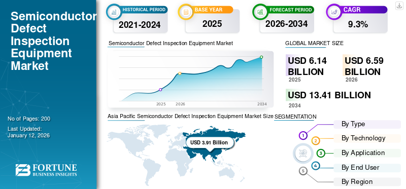
The global semiconductor defect inspection equipment market size was valued at USD 6.14 billion in 2025 and is projected to grow from USD 6.59 billion in 2026 to USD 13.41 billion by 2034, exhibiting a CAGR of 9.03% during the forecast period. Asia Pacific dominated the semiconductor defect inspection equipment market with a share of 63.07% in 2025.
Semiconductor defect inspection equipment refers to specialized tools and systems used to detect, analyze, and characterize defects in semiconductor wafers and chips during the manufacturing process of semiconductors. These machines are crucial for quality control and yield improvement in semiconductor fabrication. The main purpose of this machine is to detect pattern defects, crystal defects, and material irregularities in the semiconductor manufacturing process. The basic technologies used in the semiconductor manufacturing process include optical inspection systems, electron beams, x-ray inspection, and infrared detection.
Rising demand for semiconductors across numerous industry verticals, such as electronics, automotive, and data processing sectors, as well as surges in demand for semiconductor defect inspection equipment to detect patterns and crystals in the semiconductor manufacturing process, drives the market growth. Major players such as ASML Holding NV, Applied Materials Inc., and Hitachi High-Tech Corporation among others are engaged in introducing new equipment for the market to intensify the market competition. For instance, in February 2025, Toray Engineering Co Ltd launched a new series of Inspectra wafer inspection equipment for semiconductor industry. It can support both 2.5D and 3D packaging modes. It is compatible for 650mm square glass substrate and support high throughput capacity of inspect 40 seconds per panel. Moreover, major players engaged in adopting several key development moves to strenghthen the market competition.
An increasing complexity in devices across semiconductor manufacturing and a rising number of layers and interconnects that needs these equipment, fuels the market growth. Moreover, growth in demand for semiconductors across consumer electronics, automotive electronics, IoT devices, and data centers requires high-performance and reliable components, which necessitates advanced inspection equipment to fuel the market growth.
The COVID-19 pandemic had a significant impact on the market as supply chain disruption affected equipment manufacturing and shut down the fabrication facility temporarily. Moreover, after the COVID-19 pandemic, the demand for these equipment accelerated owing to accelerated digitalization, driving the chip demand and increasing investment in new semiconductor fabrication facilities; such factors contribute positively to the market growth.
Download Free sample to learn more about this report.
IMPACT OF TECHNOLOGY ON MARKET
Integration of Advanced Technologies to Bolster Market Growth
An integration of advanced technologies, such as artificial intelligence (AI) and machine learning (ML), has significantly improved the accuracy and efficiency of semiconductor defect inspection processes. These technologies enable real-time monitoring and analysis, which helps to identify pattern defects and rectify them during the manufacturing process of semiconductors. In addition, semiconductor devices are small in size and complex in design, which requires precise defect inspection equipment. Integration of 5G, IoT, and AI technologies in these machines enhances the demand for cutting-edge inspection equipment.
In addition, major players in the market are engaged in the manufacturing of technologically advanced defect inspection equipment. For instance, in December 2023, Hitachi High-Tech Corporation launched a new Dark Field defect inspection system, DI4600, for the semiconductor market. It was specially designed to inspect particles and detect defects on patterned wafers in semiconductor manufacturing operations. It offers features such as reduced wafer transfer time by 20% and improved productivity during wafer inspection.
MARKET DYNAMICS
SEMICONDUCTOR DEFECT INSPECTION EQUIPMENT MARKET TRENDS
Rapid Adoption of Advanced Technologies to Revolutionize the Defect Inspection Process is Fueling Market Growth
Major players engaged in the market are adopting new technological advancements, such as AI and ML, to revolutionize the inspection process by enabling automated analysis of inspection data. In addition, advancements in high-resolution imaging, such as scanning electron microscopy (SEM) and atomic force microscopy (AFM), improve the ability to detect the smallest defects on semiconductor wafers and chips. There is a growing emphasis on developing inspection equipment that ensures higher quality, is cost-effective, and energy-efficient.
For instance, in February 2024, Hitachi High Technologies Corporation developed a new Image-sensing analysis technology, Scanning Electron Microscopy (SEM), to detect Nanoscale defects occurring in the semiconductor manufacturing process. This machine uses AI technology to solve the issue of device scaling, which contributes towards productivity improvement and quality control.
Market Drivers
Rising Advancements in Semiconductor Technology to Fuel Market Growth
As semiconductor devices become more intricate with smaller feature sizes and advanced structures, the need for precise inspection equipment drives the market growth. Technologies, such as 5G, IoT, and AI demand highly reliable semiconductor devices. Moreover, an increasing demand for high-quality semiconductor defect inspection equipment drives the market growth.
In addition, these technologies are enhancing the chip design and manufacturing processes, which leads to more efficient and powerful semiconductors. For instance, in September 2024, the government of India invested around USD 10 billion in the government initiative named India Semiconductor Mission, which bolstered the market growth.
Download Free sample to learn more about this report.
Market Restraints
High Capital Investment Costs to Restrict Market Growth
Semiconductor defect inspection equipment is highly expensive and necessitates a significant capital investment. Thus, the variable prices of these machines hinder market development. This is majorly due to the challenges that major companies encounter while sourcing raw materials. In addition, the prices of these systems typically range from USD 2 billion to USD 5 billion, making it difficult to adopt by businesses, particularly small and medium-sized enterprises. These factors comprehensively limit the market growth.
Market Opportunities
Increasing Demand for Consumer Electronics to Provide Lucrative Opportunities for Market Growth
The growing proliferation of smartphones, laptops, wearable devices, and consumer electronics has led to increased semiconductor production. This factor enhances the demand for advanced defect inspection equipment to enhance quality control measures.
In addition, growing investments in the consumer electronics sector across the globe provide lucrative opportunities for market growth. For instance, according to Reuters, semiconductor manufacturers are anticipated to invest around USD 400 billion in semiconductor manufacturing from 2025 to 2027.
SEGMENTATION ANALYSIS
By Type
Wafer Inspection Systems Dominated the Market owing to Rising Demand for Advanced Semiconductor Devices
Based on type, the market is classified into wafer inspection systems, mask inspection systems, reticle inspection systems, and package inspection systems.
Wafer inspection systems segment is anticipated to hold a dominant market share of 43.25% in 2026. They are projected to grow at the highest growth rate during the forecast period, owing to rising demand for advanced semiconductor devices and the growing adoption of AI and ML technologies in defect inspection. In addition, growing production of semiconductor wafers for the automotive, electronics, and industrial sectors also contributes to the dominance of the segment.
Mask inspection and reticle inspection are anticipated to grow steadily during the forecast period owing to the rising complexity of integrated circuits and the continuous improvement of the semiconductor manufacturing process. In addition, rising demand for semiconductors from numerous industry verticals, which enhances the demand for such equipment for detect defects in integrated circuits, and memory devices, fuels the market growth.
The package inspection system is anticipated to grow decently during the forecast period, owing to factors such as rising demand for advanced semiconductor devices, and continuous advancements in semiconductor manufacturing technologies. All such factors boost the market growth.
To know how our report can help streamline your business, Speak to Analyst
By Technology
Optical Inspection Set to Observe Significant Growth Due to Rising Demand for High-Throughput Manufacturing
Based on technology, the market is segmented into optical inspection, E-beam inspection, X-ray inspection, and UV & infrared inspection.
The Optical inspection segment is expected to account for 52.96% of the market in 2026. It is projected to grow at the highest growth rate during the forecast period due to factors such as rising demand for such technology for semiconductor manufacturing, consumer electronics, automotive electronics, and medical devices. In addition, the rising complexity of manufacturing processes and the need for high precision and reliability also drive the growth of this segment in the market.
The E-beam inspection segment is projected to grow steadily with a CAGR of 8.60% during the forecast period (2025-2032), owing to the shrinking size of semiconductor devices and rising adoption of EUV lithography technologies. Moreover, the rising adoption of this technology, which offers higher throughput and improved defect detection, bolsters the segment’s growth.
The X-ray defect inspection segment is anticipated to grow at a decent rate during the forecast period owing to growing innovation in imaging techniques and higher-resolution detectors, which enhance the demand for such technologies and bolster the market's growth.
The UV and infrared detection segment is projected to grow decently during the forecast period, owing to factors such as the moderate adoption of industry 4.0 technologies such as AI and IoT integration. These technologies enable real-time monitoring and data analysis, which improves efficiency and product quality.
By Application
Integrated Circuits Dominated the Market Owing to Rising Demand from Semiconductor and Automotive Electronics
Based on application, the market is classified into integrated circuits, memory devices, light emitting diodes (LED), and Micro-electromechanical systems.
he Integrated circuits segment is estimated to attain 44.16% of the market share in 2026 and are projected to grow at the highest growth during the forecast period. This is due to the rising demand for high-performance integrated circuits across semiconductors and automotive electronics, which subsequently raises the demand for defect inspection equipment and uplifts market growth. T
Memory devices and light-emitting diodes (LED) are anticipated to grow steadily with a CAGR of 8.70% during the forecast period (2025-2032), owing to increasing complexity in semiconductor design patterns. These patterns require advanced inspection tools such as e-beam inspection and optical inspection systems to bolster the market's growth.
Micro-electromechanical systems are projected to grow decently during the forecast period, owing to factors such as the rising demand for MEMS devices in various sectors such as electronics, healthcare, and industrial.
By End User
Integrated Device Manufacturers Dominate the Market Due to Rising Demand for ICs from Various End Use Industries
Based on end-user, the market segments into integrated device manufacturers, semiconductor foundries, and test home.
The integrated device manufacturers segment is poised to acquire 48.41% of the market share in 2026 and are projected to grow at the highest rate during the forecast period. Rising demand for defect inspection equipment for numerous industry verticals such as automotive, and consumer electronics sector, fuels market growth.
The semiconductor foundries segment is expected to dominate the market due to the growing need for semiconductors from end-users such as medical devices, electronics, and automotive sectors, which fuels the market growth. This segment is foreseen to grow with a considerable CAGR of 8.50% during the forecast period (2025-2032).
The test home segment is anticipated to experience decent growth during the forecast period owing to an increase in awareness about the testing of semiconductors and their components. In addition, strict government regulations concerning the testing of devices are likely to drive the semiconductor defect inspection equipment market growth.
SEMICONDUCTOR DEFECT INSPECTION EQUIPMENT MARKET REGIONAL OUTLOOK
The market covers five major regions, mainly North America, Europe, Asia Pacific, Middle East & Africa, and South America.
ASIA PACIFIC
Asia Pacific Semiconductor Defect Inspection Equipment Market Size, 2025 (USD Billion)
To get more information on the regional analysis of this market, Download Free sample
Asia Pacific accounted for USD 3.91 billion in 2025, representing 63.70% of the global market share, and is projected to reach USD 4.22 billion in 2026. Growth in consumer electronics and smart home devices has enhanced the demand for semiconductor defect inspection equipment. In addition, government investment in the construction of new semiconductor manufacturing plants across China, India, and Japan, among others, enhances the demand for efficient defect inspection equipment and drives market growth in the region. For instance, according to InvestKorea, the South Korean government planned to invest around USD 450 billion to build a semiconductor industry supply chain across South Korea. These factors drive the growth of the semiconductor defect inspection equipment market in the Asia Pacific Region. India is estimated to acquire USD 0.23 billion in 2026, while Japan is foreseen to hold USD 1.10 billion in the same year.
China Dominates the Market Attributing to the Adoption of Technological Advancements in Products
China is one of the largest consumers of semiconductors and related products. Rising demand for silicon wafers from various end users, such as consumer electronics, smart devices, electric vehicles, and the automotive sector, enhances the demand for efficient defect inspection equipment. In addition, growing adoption of AI and ML in defect inspection equipment which bolster the growth of the market. China is anticipated to be worth USD 1.79 billion in 2026.
To know how our report can help streamline your business, Speak to Analyst
Europe
Europe contributed 13.00% to the global market in 2025, with a valuation of USD 0.8 billion, and is projected to reach USD 0.86 billion in 2026. The market for semiconductor defect inspection equipment in Europe is set to experience substantial growth during the forecast period, driven by advancements in defect inspection technology and rising demand for high-quality semiconductors. The U.K. market continues oAs manufacturers work to satisfy the changing requirements of different industries, the significance of cutting-edge inspection technologies is growing. This has led to the growing adoption of semiconductor defect inspection machinery across Europe. Germany is expected to gain USD 0.26 billion in 2026, while France is poised to hold USD 0.11 billion in 2025.
North America
The North America market generated USD 1.03 billion in 2025, representing 16.80% of the global market landscape, and is expected to reach USD 1.1 billion in 2026. The North American market is projected to grow moderately during the forecast period due to factors such as the strong presence of key players, such as KLA Corporation, Applied Materials, Hitachi High Technologies, and ASML, among others, which helps to improve the product portfolio of such equipment and drive the market growth. Moreover, there is a growing demand for integrated circuits and semiconductor wafers across industries such as electronics and automotive. For instance, according to the Semiconductor Industry Association, in October 2024, the U.S. government planned to invest around USD 450 billion in semiconductor plants.
The U.S. market is projected to grow at a moderate growth rate during the forecast period owing to factors such as rising adoption of industry 4.0 technologies such as AI, IoT, and Machine learning, which fuels the adoption of precise and reliable inspection equipment. The U.S. market is poised to be worth USD 0.78 billion in 2025.
Middle East & Africa
In 2025, Middle East & Africa held 3.60% of the global market, reaching a valuation of USD 0.22 billion, and is projected to grow to USD 0.23 billion in 2026. The region is projected to grow moderately during the forecast period, owing to countries such as Saudi Arabia, Egypt, and the UAE emerging as key players due to their investments in renewable energy and consumer electronics. This drives the demand for advanced semiconductor technologies, leading to the growth of the market in the region. The GCC market is set to acquire USD 0.1 billion in 2025.
Latin America
Latin America contributed approximately USD 0.18 billion to the global market in 2025, accounting for 2.90% share, and is expected to reach USD 0.18 billion in 2026.
COMPETITIVE LANDSCAPE
Key Industry Players
Major Players Implement Acquisition, Product Launch, and Agreement as Key Developmental Strategies to Intensify the Market Competition
Market players, such as ASML Holding NV, Applied Materials Inc., and Hitachi High-Tech Corporation, among others, engaged in offering product launches, agreements, and acquisitions as key development strategies to strengthen the market competition and also to improve their geographical presence. For instance, in March 2024, Hitachi High-Tech Corporation introduced a new LS9300AD inspection system used to detect defects in the front as well as the back side of pattern semiconductor wafers. It has features, such as reduced inspection cost, improved throughput detection, and high sensitivity.
List of Key Semiconductor Defect Inspection Equipment Companies Profiled
- KLA Corporation (U.S.)
- Applied Materials (U.S.)
- ASML Holding (Netherlands)
- Onto Innovations Inc (U.S.)
- JEOL Ltd (Japan)
- Lasertech Corporation (Japan)
- NIKON (Japan)
- Veeco Instruments Inc (U.S.)
- Hitachi High Technologies Corporation (Japan)
- Screen Holdings Co. Ltd (Japan)
- Onto Innovation (U.S.)
- Olympus Corporation (Japan)
- Microtronic Inc (U.S.)
- Naura Technology Group (China)
- Bruker Corporation (U.S.)
- Nova Measuring Instruments Ltd (Israel)
KEY INDUSTRY DEVELOPMENTS
- October 2024: Onto Innovations Inc. acquired Lumina Instruments Inc., based in Milpitas, California, U.S., and deals in semiconductor wafer defect inspection equipment. The acquisition was done for around USD 250 million. The main purpose of the acquisition was to improve the production capacity of inspection equipment.
- September 2024: Lasertech Corporation launched a new SICA 108 semiconductor wafer inspection and review system for the semiconductor market. It has features such as high speed in operation and high sensitivity, and it is enabled with smart technologies such as automated guided vehicles and overhead hoist transports.
- December 2023: Hitachi High-Tech Corporation launched a new DI2800 defect inspection equipment. It is a cutting-edge metrology system that can support semiconductor wafers upto 8 inches (200 mm). It offers features such as ensuring safety and high speed of operation.
- May 2023: KLA Corporation introduced a new Voyager 1035 defect inspection equipment for the semiconductor market. It uses a DefectWise deep learning algorithm to detect defects and improve the inspection capacity by 30%. This machine is used in the inspection of photoresist layers in applications such as developing inspection and photocell monitoring devices.
- December 2022: Applied Material Inc. launched a new Cold Field Emission defect inspection equipment that can support the e-beam system and can operate under 1,5000 C. The company launched the SEMVISISION G10 defect review system and Primevision 10 defect inspection equipment for semiconductors and related markets. It has features that are 10 times faster than other inspection systems.
REPORT COVERAGE
The global semiconductor defect inspection equipment market report provides a detailed analysis of the market. It focuses on key aspects such as leading companies, type, technology, application, and end users of the product. Besides, the report offers insights into the market trends and highlights key industry developments. In addition to the factors above, the report encompasses several factors that contributed to the growth of the market in recent years.
Request for Customization to gain extensive market insights.
Report Scope and Segmentation
|
ATTRIBUTE |
DETAILS |
|
|
Study Period |
2021-2034 |
|
|
Base Year |
2025 |
|
|
Forecast Period |
2026-2034 |
|
|
Historical Period |
2021-2024 |
|
|
Growth Rate |
CAGR of 9.3% from 2026 to 2034 |
|
|
Unit |
Value (USD Billion) |
|
|
Segmentation |
By Type, By Technology, By Application, By End User, and By Region |
|
|
Segmentation |
By Type
By Technology
By Application
By End User
By Region
|
|
|
Key Market Players Profiles in the Report |
KLA Corporation (U.S.), Applied Materials (U.S.), ASML Holding (Netherlands), Onto Innovations Inc (U.S.), JEOL Ltd (Japan), Lasertech Corporation (Japan), NIKON (Japan), Veeco Instruments Inc (U.S.), Hitachi High Technologies Corporation (Japan), and Screen Holdings Co. Ltd (Japan). |
|
Frequently Asked Questions
As per a Fortune Business Insights study, the market was valued at USD 6.59 billion in 2026.
By 2032, the market is expected to reach USD 10.94 billion.
The market is projected to grow at a compound annual growth rate (CAGR) of 9.3% during the forecast period.
The wafer inspection system segment is expected to lead the market over the forecast period.
Rising advancements in semiconductor technology fuel the market growth.
KLA Corporation, Applied Materials, ASML Holding, Onto Innovations Inc., JEOL Ltd, Lasertech Corporation, NIKON, Veeco Instruments Inc., Hitachi High Technologies Corporation, and Screen Holdings Co. Ltd are the leading companies in this market.
Asia Pacific dominated the semiconductor defect inspection equipment market with a share of 63.07% in 2025.
Technological advancements and integration with Industry 4.0 fuels market growth.
Based on end user, the integrated device manufacturers segment is projected to lead the market.


- 2021-2034
- 2025
- 2021-2024
- 200
Get 30-60 hrs Free Customization
Expand Regional and Country Coverage, Segments Analysis, Company Profiles, Competitive Benchmarking, and End-user Insights.
Related Reports
-
US +1 833 909 2966 ( Toll Free )
-
Get In Touch With Us