Semiconductor Metrology and Inspection Equipment Market Size, Share & Industry Analysis, By Type (Optical and Beam), By Technology (Wafer Inspection System, Mask Inspection System, Thin Film Metrology, Package Inspection, and Others), By Dimension (2D Metrology/Inspection, 3D Metrology/Inspection, and Hybrid 2D/3D Systems), By End-User (Foundries, Integrated Device Manufacturing (IDM) Firms, Outsourced Semiconductor Assembly and Test (OSAT) Companies, and Others), and Regional Forecast, 2026 – 2034

(Offer valid till 15th Jul 2026)
SEMICONDUCTOR METROLOGY AND INSPECTION EQUIPMENT MARKET SIZE AND FUTURE OUTLOOK
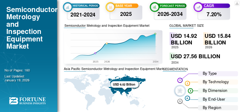
The global semiconductor metrology and inspection equipment market size was valued at USD 15.26 billion in 2025. The market is projected to grow from USD 16.26 billion in 2026 to USD 29.57 billion by 2034, exhibiting a CAGR of 7.8% during the forecast period. Asia Pacific dominated the semiconductor metrology and inspection equipment market with a market share of 34.4% in 2025.
Semiconductor metrology and inspection equipment is a category of tools that are used in the production of semiconductor chips to measure physical dimensions, material properties, and alignment accuracy of semiconductor wafers. The equipment can also be used to detect defects at different stages in the manufacturing process. Moreover, the rising complexity of semiconductor designs and manufacturing processes is driving demand for advanced metrology and inspection equipment to ensure precision, minimize defects, and maintain high yield, a key factor behind market growth.
Key players in the market include KLA Corporation, Applied Materials, Inc., Hitachi High-Tech Corporation, Onto Innovation, Inc., and Nova Ltd. They are heavily investing in R&D to develop high-precision inspection and metrology systems capable of addressing challenges at advanced nodes.
Download Free sample to learn more about this report.
SEMICONDUCTOR METROLOGY AND INSPECTION EQUIPMENT MARKET TRENDS
Rising Adoption of AI-Driven Inspection and Analytics Enhances Market Growth
A growing shift toward integrating artificial intelligence (AI) and machine learning (ML) into inspection and process control workflows is boosting the semiconductor metrology and inspection equipment market growth. As semiconductor manufacturing becomes even more complex, with the amount of data produced on the manufacturing floor, traditional rule-based inspection systems are insufficient to handle the large volume of data generated by high-volume production over time.
AI-based solutions can find defects more accurately by learning from large datasets, recognizing patterns, and separating nuisance defects from those that affect yield. The net effect of this will be a large reduction in false-positive rates while providing manufacturers with improved decision-making accuracy regarding manufacturing efficiency. For instance,
- In February 2026, Siemens acquired Canopus AI to integrate AI-driven metrology and inspection into its semiconductor manufacturing solutions. Canopus AI’s technology enables precise wafer and mask inspection, improving edge placement error measurement, yield, and process control.
As a result, AI-driven inspection and analytics are becoming a key differentiator for equipment providers, enabling them to deliver higher value through intelligent, data-centric solutions.
MARKET DYNAMICS
MARKET DRIVERS
Download Free sample to learn more about this report.
Rising Need for Defect-Free Manufacturing and Advanced Process Control to Propel Market Expansion
The growing deployment of high-performance computing processors, AI accelerators, GPUs, network processors, and advanced memory devices is significantly increasing the precision and reliability requirements of semiconductor manufacturing. All of these chip types are intended to support data-intensive and performance-critical workloads, meaning there is virtually zero tolerance for defects, variance, and/or drift. If a chip has even a small defect, it can diminish overall chip efficiency, affect thermal performance, and/or cause chip failure; therefore, manufacturers are required to produce defect-free chips through tight manufacturing processes.
As device complexity continues to increase, these tools are becoming increasingly crucial for quality assurance and for maintaining production effectiveness and yield in high-dollar chip manufacturing facilities. In addition, the need for AI Infrastructure continues to rise, further supporting this driver. For instance,
- NVIDIA reported fiscal 2026 full-year revenue of USD 215.9 billion, up 65% year over year, while its Data Center revenue reached USD 62.3 billion in the fourth quarter, up 75% year over year. This reflects the sharp increase in demand for AI computing hardware, which in turn is raising production volumes for advanced GPUs and accelerator platforms.
Together, these developments indicate that the rising production of high-performance and AI-oriented semiconductors is intensifying the need for highly accurate inspection and metrology solutions to support yield, reliability, and large-scale manufacturing efficiency.
MARKET RESTRAINTS
High Dependence on Semiconductor Capex Cycles to Limit Market Growth
Semiconductor inspection equipment relies heavily on semiconductor manufacturers' capital spending cycles. Primarily, semiconductor manufacturers buy these products when they are expanding their fabs, adding capacity, or transitioning to a new technology node. Unlike consumables and process materials, which are bought repeatedly, metrology and inspection equipment is capital equipment with a long purchase cycle. Therefore, the timing of equipment purchases closely aligns with the strategic capital expenditure plans of foundries and integrated device manufacturers.
Expansion in semiconductor equipment spending occurs when demand for semiconductor manufacturing capacity is strong, such as during node transitions or ramp-ups in manufacturing volume across the logic or memory segments. Conversely, during periods of declining demand, such as when semiconductor companies are correcting inventories or experiencing weak demand in their end markets, these customers reduce or defer capital expenditures, thereby directly impacting order receipt levels at suppliers of semiconductor equipment.
MARKET OPPORTUNITIES
Advanced Node Migration Driving Demand for High-Precision Metrology and Inspection Solutions
Transitioning to advanced semiconductor technology nodes, such as 3nm and 2nm, will provide an enormous opportunity for companies producing metrology and inspection equipment due to the increase in pattern defects, overlay errors, line edge roughness, and process variability that occur with the reduced geometric sizes and more complex architectures of the devices being manufactured at these nodes. At these nodes, semiconductor manufacturers face challenges beyond device miniaturization, including increasingly advanced architectures and the integration of diverse materials in the manufacturing process.
- TSMC stated in its 2024 annual report that its 2nm (N2) technology uses its first-generation nanosheet transistor technology and is expected to enter volume production in the second half of 2025, while its 3nm (N3) technology was already in its third year of volume production in 2024.
As nodes scale, the number of inspection and measurement steps has increased, and the precision required has also increased. Increased tool intensity and reliance on advanced metrology solutions will continue to be driven by the growing number of inspection and measurement steps in wafer fabrication facilities. Advanced node migration has created sustained demand for and growth opportunities for metrology and inspection equipment manufacturers.
Segmentation Analysis
By Type
Optical Segment Led Market as It Offers High-resolution and Non-destructive Inspection
Based on the type, the market is bifurcated into optical and beam.
The optical segment held the largest market share in 2025. This is owing to its ability to provide high-resolution, non-destructive inspection, which is critical for detecting defects in advanced semiconductor nodes. As demand for smaller, more complex devices continues to increase, optical inspection techniques remain the best and most widely used method for providing quality assurance throughout the semiconductor manufacturing process.
The beam segment is anticipated to grow at the highest compound annual growth rate (CAGR) of 9.6% over the forecast period. This is owing to its superior precision and ability to handle complex semiconductor structures, making it essential for advanced node development and defect detection.
By Technology
Precision and Defect Detection Advancements Led to Dominance of Wafer Inspection Systems
Based on the technology, the market is divided into wafer inspection system, mask inspection system, thin film metrology, package inspection, and others (probe card inspection, lithography metrology, etc.).
The wafer inspection system segment held the largest market share in 2025 and is expected to grow at the highest CAGR of 9.1% during the forecast period. This is owing to its critical role in detecting defects early in the semiconductor manufacturing process, ensuring high yields. The use of wafer inspection systems is anticipated to become even more essential for proper process control and quality assurance as semiconductor nodes shrink across logic, memory, and advanced packaging applications.
The package inspection segment is anticipated to grow at a moderate CAGR of 7.9% over the forecast period. This is owing to the increasing complexity of semiconductor packages and the need for accurate defect detection in advanced packaging technologies.
By Dimension
Accuracy and Speed to Enhance the Leadership of 2D Metrology/Inspection in Market
Based on the dimension, the market is categorized into 2D metrology/inspection, 3D metrology/inspection, and hybrid 2D/3D Systems.
2D metrology/inspection is anticipated to account for the largest market share. This is owing to the extensive application of ensuring the dimensional accuracy and quality of semiconductor devices throughout the manufacturing process, particularly in the initial stages. Two-dimensional technologies enable quick inspection and measurement of critical dimensions, making them the solution of choice for high-volume production processes.
3D metrology/inspection is anticipated to grow at the highest CAGR of 9.4% over the forecast period. This is owing to its increasing importance in measuring and inspecting complex, multi-dimensional semiconductor structures, particularly in advanced packaging and 3D integration.
By End-user
To know how our report can help streamline your business, Speak to Analyst
Rising Demand for Advanced Semiconductor Nodes Boosted Foundries Segment Growth
Based on the end-user, the market is classified into foundries, integrated device manufacturing (IDM) firms, outsourced semiconductor assembly and test (OSAT) companies, and others (R&D labs, memory makers, etc.).
Foundries held the dominating market share in 2025. This is owing to their central role in semiconductor manufacturing, especially as the demand for advanced nodes and process technologies continues to rise. As foundries serve a wide range of industries, their need for advanced metrology and inspection equipment to ensure high yields and precision is driving significant market growth.
Outsourced semiconductor assembly and test (OSAT) companies are anticipated to grow at the highest CAGR of 9.7% during the forecast period. This is owing to the increasing complexity of semiconductor packages and the growing demand for advanced packaging solutions across various industries.
Semiconductor Metrology and Inspection Equipment Market Regional Outlook
By geography, the market is categorized into North America, South America, Europe, the Middle East & Africa, and Asia Pacific.
Asia Pacific
Asia Pacific Semiconductor Metrology and Inspection Equipment Market Size, 2025 (USD Billion)
To get more information on the regional analysis of this market, Download Free sample
Asia Pacific accounted for the largest semiconductor metrology and inspection equipment market share in 2024, valued at USD 5.88 billion, and maintained that lead in 2025, with USD 6.25 billion. The region dominates the market due to its strong concentration of semiconductor manufacturing capacity and capital investment. The majority of foundries, memory manufacturing companies, and semiconductor fabrication facilities use semiconductor inspection equipment for ongoing inspections and measurements through multiple production phases. This accumulation of production activity generates a continuous demand for highly accurate process control tools within this area, making it the main contributor to revenue in the global semiconductor manufacturing (and value-added) market.
For instance,
- In May 2024, TrendForce reported that NVIDIA and AMD fully booked TSMC’s advanced packaging capacity through 2025, and that its CoWoS monthly capacity was expected to increase from around 15,000 units in 2023 to 45,000–50,000 units by the end of 2024.
China Semiconductor Metrology and Inspection Equipment Market
The Chinese market is projected to be one of the largest globally, with 2026 revenues estimated at around USD 2.43 billion, roughly 14.9% of global sales.
To know how our report can help streamline your business, Speak to Analyst
Japan Semiconductor Metrology and Inspection Equipment Market
The Japanese market in 2026 is estimated at around USD 1.48 billion, accounting for roughly 9.1% of global revenues. This is due to significant investments in semiconductor manufacturing, particularly in advanced packaging and memory, supported by government initiatives and the country's strong semiconductor production capabilities.
India Semiconductor Metrology and Inspection Equipment Market
The Indian market in 2026 is estimated at around USD 0.92 billion, accounting for roughly 5.7% of global revenues.
North America
North America is estimated to reach USD 5.03 billion in 2026 and secure the position of the second-largest region in the market. This is owing to its dominance in several sectors of semiconductor equipment production, its innovations in process control, and its development of advanced chips. The fact that leading producers of semiconductor equipment are either located or are headquartered in North America helps reinforce the local implementation of high-value metrology and inspection instruments. High revenues generated by the semiconductor industry, along with ongoing support through continued capital spending and a commitment to manufacturing more products domestically, are also attributes that the North American semiconductor industry needs to sustain its growth. For instance,
- In July 2025, the Semiconductor Industry Association stated that the U.S. semiconductor industry commanded just over 50% of global chip revenues. This reflects North America’s strong technology base and reinforces its position as the second-largest market.
U.S. Semiconductor Metrology and Inspection Equipment Market
Given North America’s significant contribution and the U.S. dominance in the region, the U.S. market can be estimated at around USD 3.68 billion in 2026, accounting for 22.6% of global sales.
Europe
Europe is projected to grow at a CAGR of 8.4% over the coming years, the highest among all regions, and reach a valuation of USD 3.01 billion in 2026. The growth of the European market is mainly driven by increasing demand for advanced semiconductor manufacturing technologies across industries such as automotive, aerospace, and industrial automation. In addition, there is strong government support through regulation, with the EU's Digital Compass plan pushing for increased semiconductor self-sufficiency and enhancing local manufacturing capabilities. For instance,
- The European Union (EU) aims to produce 20% of the world’s semiconductors by 2030, with a focus on enhancing local chip production.
U.K. Semiconductor Metrology and Inspection Equipment Market
The U.K. market in 2026 is estimated at around USD 0.64 billion, representing roughly 3.9% of global revenues.
Germany Semiconductor Metrology and Inspection Equipment Market
Germany's market size is projected to reach approximately USD 0.59 billion in 2026, equivalent to around 3.6% of global sales.
South America
South America is expected to witness moderate growth in this market space during the forecast period. The South America market is set to reach a valuation of USD 0.56 billion in 2026. Market growth in South America is driven by increasing demand for semiconductors across the consumer electronics, automotive, and telecommunications sectors, as well as by growing investments in semiconductor manufacturing infrastructure.
Middle East & Africa
The Middle East & Africa region is estimated to reach USD 0.98 billion in 2026 and is expected to grow at a prominent rate in the coming years. Market growth in the Middle East & Africa is driven by increasing government investments in digital infrastructure and technology, particularly in smart cities and industrial automation projects. Additionally, the rapid growth of the Consumer Electronics and automotive industries in this region has increased demand for advanced semiconductors, leading to a greater need for metrology and inspection equipment. In the Middle East & Africa, the GCC is set to reach USD 0.39 billion in 2026.
COMPETITIVE LANDSCAPE
Key Industry Players
Focus on Expanding Advanced Manufacturing Capabilities by Key Players to Propel Market Growth
The global semiconductor metrology and inspection equipment market has a semi-consolidated structure, with prominent players such as KLA Corporation, Applied Materials, Inc., Hitachi High-Tech Corporation, Onto Innovation, Inc., and Nova Ltd. holding significant positions. These companies are driving market growth through continuous investments in advanced metrology and inspection technologies, including optical and e-beam inspection, CD-SEM, overlay metrology, and defect review solutions. Strategic initiatives, such as expanding inspection capacities, enhancing defect-detection technologies, and developing next-generation process-control solutions, are enabling improved performance and higher yield efficiency across the logic, memory, advanced packaging, and automotive semiconductor sectors.
Other notable players in the global market include ASML Holding N.V., Lasertec Corporation, Thermo Fisher Scientific Inc., Camtek, and Carl Zeiss AG. These companies are increasingly focusing on strengthening their inspection capabilities, optimizing manufacturing processes, and scaling production capacity to meet rising demand. Expansion into new regional markets and the development of cutting-edge inspection systems for emerging technologies, such as 3D NAND and advanced packaging, are expected to reinforce their market positioning and support sustained market growth throughout the forecast period.
LIST OF KEY SEMICONDUCTOR METROLOGY AND INSPECTION EQUIPMENT COMPANIES PROFILED
- KLA Corporation (U.S.)
- Applied Materials, Inc. (U.S.)
- Onto Innovation, Inc. (U.S.)
- Carl Zeiss AG (Germany)
- ASML Holding N.V. (Netherlands)
- Camtek Ltd. (Israel)
- Hitachi High-Tech Corporation (Japan)
- Lasertec Corporation (Japan)
- Nova Ltd. (Israel)
- Thermo Fisher Scientific Inc. (U.S.)
KEY INDUSTRY DEVELOPMENTS
- February 2026: Applied Materials, Inc. unveiled transistor and wiring innovations for faster AI chips, positioning the announcement as a technology advance for next-generation semiconductor performance.
- January 2026: KLA expanded its global footprint by opening a new R&D and innovation hub in India, focusing on AI, software, and advanced process control technologies to support semiconductor customers.
- November 2025: Onto Innovation, Inc. completed the acquisition of selected Semilab product lines for materials composition and electrical analysis, strengthening its portfolio in advanced logic, memory, specialty devices, and advanced packaging.
- October 2025: Hitachi High Tech Corporation launched the SU9600, a next-generation ultrahigh-resolution scanning electron microscope with higher throughput, aimed at supporting semiconductor R&D and process control as AI-driven device complexity increases.
- September 2025: ZEISS Group introduced the new AIMS EUV 3.0 platform, a next-generation mask qualification system designed to support both Low-NA and High-NA EUV roadmaps, with the company stating the new generation triples mask throughput.
- April 2025: Applied Materials, Inc. announced a strategic investment in BE Semiconductor Industries (Besi), purchasing 9% of outstanding shares to build on collaboration in hybrid bonding technology for advanced packaging.
- March 2025: ASML Holding N.V. signed a new five-year strategic partnership with imec, focused on semiconductor research and sustainability, bringing together both companies’ expertise to support future semiconductor innovation.
REPORT COVERAGE
The global semiconductor metrology and inspection equipment market analysis includes a comprehensive study of the market size & forecast across all market segments covered in the report. It includes details on the market dynamics and market trends expected to drive the market over the forecast period. It provides information on key aspects, including technological advancements, pipeline candidates, the regulatory environment, and product launches. Additionally, it details partnerships, mergers & acquisitions, key industry developments, and prevalence by key regions. The global market research report also provides a detailed competitive landscape, including market share and profiles of key players.
Request for Customization to gain extensive market insights.
Report Scope & Segmentation
| ATTRIBUTE | DETAILS |
| Study Period | 2021-2034 |
| Base Year | 2025 |
| Estimated Year | 2026 |
| Forecast Period | 2026-2034 |
| Historical Period | 2021-2024 |
| Growth Rate | CAGR of 7.8% from 2026 to 2034 |
| Unit | Value (USD Billion) |
| Segmentation | By Type, Technology, Dimension, End-User, and Region |
| By Type |
|
| By Technology |
|
| By Dimension |
|
| By End-User |
|
| By Region |
|
Frequently Asked Questions
According to Fortune Business Insights, the global market value stood at USD 15.26 billion in 2025 and is projected to reach USD 29.57 billion by 2034.
In 2025, the market value in Asia Pacific stood at USD 6.25 billion.
The market is projected to grow at a CAGR of 7.8% during the forecast period of 2026-2034.
By end-user, the foundries segment led the market in 2025.
Rising need for defect-free manufacturing and advanced process control to propel market expansion.
KLA Corporation, Applied Materials, Inc., Hitachi High-Tech Corporation, Onto Innovation, Inc., and Nova Ltd. are the major players in the global market.
Asia Pacific dominated the market in 2025.


- 2021-2034
- 2025
- 2021-2024
- 215
-
(Offer valid till 15th Jul 2026)
Get 30-60 hrs Free Customization
Expand Regional and Country Coverage, Segments Analysis, Company Profiles, Competitive Benchmarking, and End-user Insights.
Related Reports
-
US +1 833 909 2966 ( Toll Free )
-
Get In Touch With Us