Wafer Level Packaging Market Size, Share & Industry Analysis, By Type (3D TSV WLP, 2.5D TSV WLP, Wafer Level Chip Scale Packaging (WLCSP), Nano WLP), By Technology (Fan-in Wafer Level Packaging (FI-WLP) and Fan-out Wafer Level Packaging (FO-WLP)), By End Use (Consumer Electronics, IT & Telecommunication, Automotive, Healthcare, and Others), and Regional Forecast, 2026-2034
Wafer Level Packaging Market Size & Industry Overview
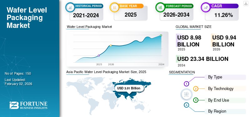
The global wafer level packaging market size was valued at USD 8.98 billion in 2025. The market is projected to grow from USD 9.94 billion in 2026 to USD 23.34 billion by 2034, exhibiting a CAGR of 11.26% during the forecast period. Asia Pacific dominated the wafer level packaging market with a market share of 33.53% in 2025.
Wafer-level packaging (WLP) is a semiconductor packaging method that involves packaging integrated circuits (ICs) directly at the wafer stage, prior to the dicing of the wafer into separate chips. In contrast to conventional packaging, which requires the chips to be separated before packaging, WLP constructs interconnects, protective layers, and occasionally redistribution layers (RDLs). At the same time, the ICs remain part of the wafer. This technique facilitates the creation of smaller, thinner, and more efficient packages, making it ideal for high performance and compact electronic devices.
Furthermore, the market encompasses several key players Amkor Technology, Taiwan Semiconductor Manufacturing Company Limited, and Nordson Corporation, at the forefront. Broad portfolio with innovative product launch, and strong geographic presence expansion have supported the dominance of these companies in the global market.
Download Free sample to learn more about this report.
Wafer Level Packaging Market Key Takeaways
- 2025 Market Size: USD 8.98 billion
- 2026 Market Size: USD 9.94 billion
- 2034 Forecast Market Size: USD 23.34 billion
- CAGR: 11.26% from 2026–2034
- Asia Pacific dominated the wafer level packaging market with a 33.53% share in 2025.
- The 3D TSV WLP type segment is expected to account for 36.61% of the market in 2026.
- The fan-out wafer level packaging (FO-WLP) segment is projected to hold a 57.94% market share in 2026.
Asia Pacific
Asia Pacific led the global market with USD 3.01 billion in revenue in 2025 and is projected to reach USD 3.36 billion in 2026.
North America
North America accounted for 25.96% of the global market in 2025 and is expected to reach USD 2.58 billion in 2026.
Europe
Europe contributed 21.00% of global market revenue in 2025 and is projected to reach USD 2.08 billion in 2026.
U.S.
The market is projected to reach USD 2.08 billion by 2026, benefiting from the country's leadership in semiconductor design, innovation, and high-performance computing technologies.
Japan
The market is projected to reach USD 0.64 billion by 2026, supported by its strong semiconductor ecosystem and increasing demand for advanced packaging technologies.
Read More
MARKET DYNAMICS
MARKET DRIVERS
Rising Demand for Miniaturized and High-Performance Electronics Drives Market Growth
The increasing inclination toward compact, lightweight, and high-performance electronic devices significantly drives the global wafer level packaging market. As consumer electronics including smartphones, wearables, and IoT devices progress, manufacturers seek advanced packaging solutions capable of integrating higher functionality within smaller dimensions. Wafer level packaging provides reduced form factors, enhanced electrical performance, and superior thermal efficiency, rendering it suitable for high-density integration. Additionally, this technology facilitates lower production costs and better yield rates in comparison to conventional packaging, thereby further promoting its adoption in the consumer and automotive electronics sectors. It thus drives the global wafer level packaging market growth.
MARKET RESTRAINTS
High Initial Investment and Complex Manufacturing Process Hampers Market Growth
Despite its benefits, the wafer-level packaging market encounters limitations stemming from the substantial capital investment and technical intricacies linked to its manufacturing processes. Establishing WLP facilities necessitates sophisticated equipment, accurate wafer handling systems, and rigorous cleanroom conditions, all of which elevate the total production costs. Moreover, incorporating WLP into current semiconductor manufacturing lines requires specialized knowledge and process refinement. Small and medium-sized semiconductor manufacturers frequently struggle to adopt these technologies due to constrained financial and technical resources, potentially obstructing broader implementation.
MARKET OPPORTUNITIES
Growing Adoption in Automotive and 5G Applications Creates Lucrative Growth Opportunities
The growing integration of electronics within vehicles, along with the swift development of 5G infrastructure, offers substantial growth prospects for wafer level packaging technologies. Advanced driver-assistance systems (ADAS), electric vehicles (EVs), and connected car technologies depend on compact, high-reliability chips—domains where WLP demonstrates excellence due to its outstanding electrical performance and thermal management. Likewise, 5G base stations and devices necessitate high-frequency, low-latency chips, which further enhances the demand for WLP solutions. The increasing demand from data centers, AR/VR devices, and AI-driven edge computing systems also creates new growth opportunities for the market.
WAFER LEVEL PACKAGING MARKET TRENDS
Transition Toward Fan-Out and Heterogeneous Integration Emerge as a Market Trend
A significant trend influencing the global wafer level packaging market is the transition from conventional fan-in WLP to more advanced fan-out WLP and heterogeneous integration technologies. Fan-out packaging allows for increased input/output (I/O) density and accommodates multiple dies within a single package, making it particularly suitable for high-performance computing, AI chips, and mobile processors. Moreover, the emergence of 3D stacking and system-in-package (SiP) architectures is improving functionality while minimizing footprint. The increasing collaboration among foundries, OSATs (Outsourced Semiconductor Assembly and Test), and material suppliers is fostering innovation in WLP design and propelling the market toward more advanced, cost-effective solutions.
MARKET CHALLENGES
Yield Issues and Thermal Management Constraints Are Key Market Challenges
One of the primary challenges faced in the wafer level packaging sector is the maintenance of high yield rates throughout the manufacturing process, particularly for advanced packages that utilize large wafers and fine-pitch interconnects. Defects that occur during wafer handling or dicing can have a substantial impact on yield and profitability. Moreover, as chip densities continue to rise, the management of heat dissipation becomes increasingly intricate. While WLP offers superior thermal performance compared to traditional packaging methods, it still encounters difficulties in handling high-power applications without the implementation of additional cooling solutions. Tackling these technical challenges is essential for enhancing scalability and ensuring the reliability of next-generation semiconductor devices.
Download Free sample to learn more about this report.
Wafer Level Packaging Market Segmentation Analysis
By Type
High-Performance and Miniaturization Demands for 3D TSV WLP Boosted Segmental Growth
In terms of type, the market is categorized into 3D TSV WLP, 2.5D TSV WLP, wafer level chip scale packaging (WLCSP), and nano WLP.
The 3D TSV WLP type segment is expected to lead the market, contributing 36.61% globally in 2026. In 2025, the segment is anticipated to dominate with a 36.37% share. The 3D Through-Silicon Via (TSV) wafer level packaging segment leads the market owing to its unparalleled capability to satisfy the increasing demands for performance, density, and power efficiency in next-generation semiconductor applications. TSV-based WLP facilitates the vertical stacking of several chips or dies such as logic, memory, and sensors, interconnected via microscopic vias that are etched directly into the silicon. This architectural design significantly reduces interconnect lengths, offers advancements in semiconductor technology, leading to increased bandwidth, decreased latency, minimized power consumption, and improved signal integrity when compared to traditional 2D or fan-out configurations.
The wafer level chip scale packaging (WLCSP) type segment is expected to grow at a CAGR of 11.20% over the forecast period.
By Technology
High I/O Density and Superior Performance Features Boosted Segment’s Growth
In terms of technology, the market is categorized into fan-in wafer level packaging (FI-WLP) and
fan-out wafer level packaging (FO-WLP).
The fan-out wafer level packaging (FO-WLP) segment is anticipated to hold a dominant market share of 57.94% in 2026. In 2025, the segment is anticipated to dominate with a 58.21% share. The Fan-Out Wafer Level Packaging (FO-WLP) segment leads the wafer level packaging market owing to its capacity to provide greater input/output (I/O) density, improved electrical performance, and exceptional design flexibility when compared to conventional fan-in and wire-bond packaging methods. FO-WLP enhances the interconnects beyond the chip's footprint by embedding the die within a reconstituted wafer, facilitating additional external connections without enlarging the chip size. This advancement allows for the creation of compact, high-performance devices that are well-suited for contemporary consumer electronics, mobile processors, and high-speed communication components.
The fan-in wafer level packaging (FI-WLP) technology segment is expected to grow at a CAGR of 11.89% over the forecast period.
By End Use
Rising Demand for Compact and High-Performance Devices Drives Segmental Growth
Based on end use, the market is segmented into consumer electronics, IT & telecommunication, automotive, healthcare, and others.
To know how our report can help streamline your business, Speak to Analyst
In 2024, the global market was dominated by consumer electronics in terms of end use. Furthermore, the segment expected to account for 33.40% share in 2026. The consumer electronics sector leads the wafer level packaging (WLP) market, driven by the swift expansion of smartphones, tablets, wearables, and various portable devices that require compact, high-performance, and energy-efficient chips. WLP technology, which encompasses fan-in, fan-out, and 3D TSV types, facilitates the miniaturization of integrated circuits (ICs) while ensuring excellent electrical performance and thermal management essential criteria for contemporary consumer devices that are increasingly becoming thinner and more powerful.
Additionally, the high-volume production of consumer electronics is ideally suited to WLP’s economical wafer-level processing, which enables the simultaneous packaging of multiple chips, thereby decreasing manufacturing time and overall costs.
In addition, the automotive end use is projected to grow at a CAGR of 11.37% during the study period.
Wafer Level Packaging Market Regional Outlook
By geography, the market is categorized into Europe, North America, Asia Pacific, Latin America, and the Middle East & Africa.
ASIA PACIFIC
Asia Pacific Wafer Level Packaging Market Size, 2025 (USD Billion)
To get more information on the regional analysis of this market, Download Free sample
Asia Pacific accounted for USD 3.01 billion in 2025, representing 33.53% of the global market share, and is projected to reach USD 3.36 billion in 2026. The Asia Pacific region leads the global wafer level packaging market, with China, Japan, and other countries at the forefront. The robust semiconductor manufacturing infrastructure, the presence of key foundries such as TSMC, Samsung, and UMC, along with significant consumer electronics production centers, are pivotal in driving the demand for WLP. The increasing prevalence of 5G smartphones, Internet of Things (IoT) devices, and artificial intelligence (AI) chips has further accelerated this adoption. The Japan market is projected to reach USD 0.64 billion by 2026, the China market is projected to reach USD 1.1 billion by 2026, and the India market is projected to reach USD 0.91 billion by 2026.
In the region, India and China are both estimated to reach USD 0.81 and USD 0.98 billion each in 2025.
Other regions, such as North America and Europe, are anticipated to witness a notable growth in the coming years.
NORTH AMERICA
The North America market generated USD 2.33 billion in 2025, representing 25.96% of the global market landscape, and is expected to reach USD 2.58 billion in 2026. North America, especially the U.S., continues to be at the forefront of semiconductor design and research and development, facilitating the implementation of wafer-level packaging for high-performance computing, AI accelerators, and data center applications. Prominent fabless companies and robust partnerships between chip designers and OSATs (such as ASE, Amkor, and TSMC North America operations) persist in advancing the development of WLP, thus boosting the market growth in North America. The U.S. market is projected to reach USD 2.08 billion by 2026.
In 2025, the U.S. market is estimated to reach USD 1.88 billion.
EUROPE
Europe contributed 21.00% to the global market in 2025, with a valuation of USD 1.89 billion, and is projected to reach USD 2.08 billion in 2026. The automotive and industrial sectors significantly shape the semiconductor ecosystem in Europe. The adoption of wafer-level packaging (WLP) is rapidly increasing, driven by the growing need for sensors, power devices, and radar systems in electric and autonomous vehicles. Furthermore, the region's focus on energy efficiency and sustainability is in harmony with WLP's ability to minimize power consumption and material waste. The UK market is projected to reach USD 0.38 billion by 2026, while the Germany market is projected to reach USD 0.45 billion by 2026.
Backed by these factors, countries including the U.K. are expected to record the valuation of USD 0.34 billion, Germany to record USD 0.40 billion, and France to record USD 0.30 billion in 2025.
Over the forecast period, Latin America and the Middle East & Africa regions would witness a moderate growth in this market.
LATIN AMERICA
Latin America contributed approximately USD 0.98 billion to the global market in 2025, accounting for 11.00% share, and is expected to reach USD 1.08 billion in 2026. The Latin America market in 2025 is set to record USD 0.98 billion as its valuation. The wafer level packaging market in Latin America is presently modest yet expanding, fueled by an increasing demand for consumer electronics, smart devices, and automotive semiconductors, especially in Brazil and Mexico. The rise in imports of advanced chips for local assembly and electronics manufacturing indirectly promotes the adoption of WLP by enhancing regional supply chain integration.
MIDDLE EAST & AFRICA
In 2025, Middle East & Africa held 8.57% of the global market, reaching a valuation of USD 0.77 billion, and is projected to grow to USD 0.84 billion in 2026. In the Middle East & Africa, South Africa is set to attain the value of USD 0.22 billion in 2025. The region is currently in the early stages of the wafer level packaging market; however, it is demonstrating a growing interest driven by the digital transformation of various industries, the expansion of smart city initiatives, and defense electronics projects, particularly in the Gulf region.
COMPETITIVE LANDSCAPE
Key Industry Players
A Wide Range of Product Offerings, coupled with a Strong Distribution Network of Key Companies, Supported their Leading Position
The global wafer level packaging industry shows a semi-concentrated structure with numerous small- to mid-size companies actively operating across the globe. These players are actively involved in product innovation, strategic partnerships, and geographic expansion.
Amkor Technology, Taiwan Semiconductor Manufacturing Company Limited, and Nordson Corporation are some of the dominating players in the market. A comprehensive range of unit-dose packaging products, global presence through a strong distribution network, and collaborations with research and academic institutes are a few characteristics of these players that support their dominance.
Apart from this, other prominent players in the market include Lam Research Corporation, MKS Inc., Jiangsu Changjiang Electronics Technology Co. Ltd., and others. These companies are undertaking various strategic initiatives, such as investments in R&D and partnerships with pharmaceutical companies to enhance their market presence.
LIST OF KEY WAFER LEVEL PACKAGING COMPANIES PROFILED
- Amkor Technology (U.S.)
- Taiwan Semiconductor Manufacturing Company Limited (Taiwan)
- Nordson Corporation (U.S.)
- Lam Research Corporation (U.S.)
- MKS Inc. (U.S.)
- Jiangsu Changjiang Electronics Technology Co. Ltd. (China)
- Fujitsu (Japan)
- MacDermid Alpha Electronics Solutions (U.S.)
- Mycronic (Sweden)
- Yield Engineering Systems (YES) (U.S.)
- ASE Global (Taiwan)
- ECI Technology (U.S.)
- Evatec AG (Switzerland)
- Nanotronics (U.S.)
- Kulicke and Soffa Industries, Inc. (Singapore)
KEY INDUSTRY DEVELOPMENTS
- October 2025: ASE Technology Holding Co., Ltd. and Analog Devices, Inc. declared their strategic collaboration in Penang, Malaysia, marked by the signing of a binding Memorandum of Understanding. Pending the completion of the definitive transaction documents, ASE plans to acquire 100% of the equity of Analog Devices Sdn. Bhd., along with its manufacturing facility located in Penang.
- August 2025: Amkor Technology, Inc. revealed updated plans regarding the site of its new advanced semiconductor packaging and testing facility in Arizona. The facility is set to be built on a 104-acre plot located within the Peoria Innovation Core, situated in north Peoria, AZ. The Peoria City Council has unanimously sanctioned a land exchange and a revised development agreement, permitting Amkor to trade its previously allocated 56-acre parcel within the Five North at Vistancia community.
- October 2024: DELO introduced an innovative method for fan-out wafer-level packaging (FOWLP). The findings from its feasibility study indicate that by utilizing UV-curable molding materials in place of heat-curing alternatives, there is a significant reduction in warpage and die shift. Furthermore, this approach enhances curing time and reduces energy consumption.
- September 2020: KLA Corporation unveiled the Kronos 1190 wafer-level packaging inspection system, the ICOS F160XP die sorting and inspection system, along with the latest iteration of the ICOS T3/T7 Series for inspecting and measuring packaged integrated circuit (IC) components. These new tools feature heightened sensitivity, enhanced throughput, and state-of-the-art algorithms aimed at improving semiconductor device manufacturing during the packaging phase, tackling the challenges posed by diminishing feature sizes, three-dimensional structures, and heterogeneous integration.
- August 2019: Evatec AG announced that Evatec has supplied the latest generation of its CLUSTERLINE thin film deposition tool, which includes evaporation capabilities for SkyWater. This tool introduces unprecedented levels of thin film performance, which are essential for the production of carbon nanotubes and other emerging technologies. The CLUSTERLINE is a proven, high-volume production solution for single wafer processing, facilitating the integration of PVD (physical vapor deposition), highly ionized PVD, Soft Etch, and PECVD (plasma-enhanced chemical vapor deposition) process technologies.
REPORT COVERAGE
Request for Customization to gain extensive market insights.
Report Scope & Segmentation
| ATTRIBUTE | DETAILS |
| Study Period | 2021-2034 |
| Base Year | 2025 |
| Estimated Year | 2026 |
| Forecast Period | 2026-2034 |
| Historical Period | 2021-2024 |
| Growth Rate | CAGR of 11.26% from 2026-2034 |
| Unit | Value (USD Billion) |
| Segmentation |
By Type · 3D TSV WLP · 2.5D TSV WLP · Wafer Level Chip Scale Packaging (WLCSP) · Nano WLP By Technology · Fan-in Wafer Level Packaging (FI-WLP) · Fan-out Wafer Level Packaging (FO-WLP) By End Use · Consumer Electronics · IT & Telecommunication · Automotive · Healthcare · Others By Region · North America (By Type, Technology, End Use, and Country) o U.S. o Canada · Europe (By Type, Technology, End Use, and Country/Sub-region) o Germany o U.K. o France o Spain o Italy o Russia o Poland o Romania o Rest of Europe · Asia Pacific (By Type, Technology, End Use, and Country/Sub-region) o China o Japan o India o Australia o Southeast Asia o Rest of Asia Pacific · Latin America (By Type, Technology, End Use, and Country/Sub-region) o Brazil o Mexico o Argentina o Rest of Latin America · Middle East & Africa (By Type, Technology, End Use, and Country/Sub-region) o Saudi Arabia o UAE o Oman o South Africa o Rest of the Middle East & Africa |
Frequently Asked Questions
Fortune Business Insights says that the global market value stood at USD 8.98 billion in 2025 and is projected to reach USD 23.34 billion by 2034.
In 2025, the market value stood at USD 3.01 billion.
The market is expected to exhibit a CAGR of 11.26% during the forecast period of 2026-2034.
The fan-out wafer level packaging (FO-WLP) segment led the market by technology.
The key factors driving the market growth us the rising demand for miniaturized and high-performance electronics.
Amkor Technology, Taiwan Semiconductor Manufacturing Company Limited, Nordson Corporation, Lam Research Corporation, MKS Inc., and Jiangsu Changjiang Electronics Technology Co. Ltd. are some of the prominent players in the market.
Asia Pacific dominated the market in 2025.
High demand for wafer level packages from the consumer electronics sector is one of the factors that is expected to favor the product adoption.


- 2021-2034
- 2025
- 2021-2024
- 150
Get 30-60 hrs Free Customization
Expand Regional and Country Coverage, Segments Analysis, Company Profiles, Competitive Benchmarking, and End-user Insights.
-
US +1 833 909 2966 ( Toll Free )
-
Get In Touch With Us