Wafer Vacuum Assembling Equipment Market Size, Share & Industry Analysis, By Equipment Type (Wafer Bonding Equipment, Wafer Alignment Systems, Vacuum Handling & Transfer Systems, Wafer Packaging/Encapsulation Equipment, and Others), By End User (Semiconductor Foundries, Integrated Device Manufacturers (IDMs), OSAT, MEMS & Sensors Manufacturers, and Power Electronics), By Wafer Size (Below 200mm, 200–300mm, and Above 300mm), and Regional Forecast, 2026–2034
Wafer Vacuum Assembling Equipment Market Size and Future Outlook
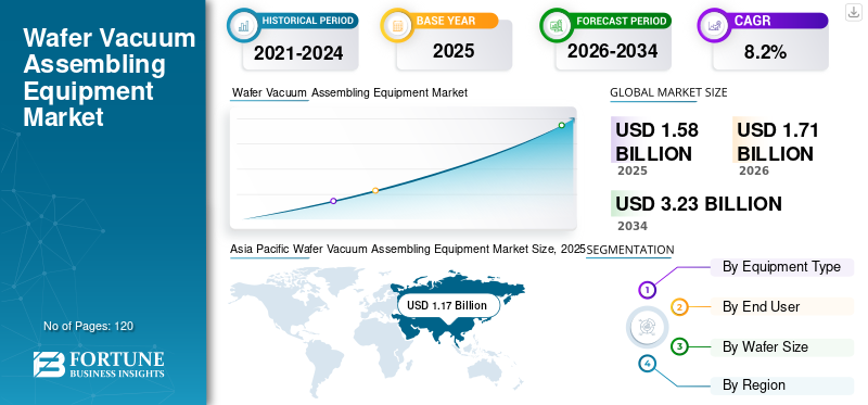
The global wafer vacuum assembling equipment market size was valued at USD 1.58 billion in 2025. The market is projected to grow from USD 1.71 billion in 2026 to USD 3.23 billion by 2034, exhibiting a CAGR of 8.2% during the forecast period. Asia Pacific dominated the wafer vacuum assembling equipment market with a market share of 72.15% in 2025.
Wafer vacuum assembling equipment refers to advanced semiconductor manufacturing systems used for wafer bonding, alignment, vacuum handling, encapsulation, and transfer processes under controlled vacuum environments. These systems are critical for ensuring precision, contamination control, and structural integrity in semiconductor device fabrication.
The market is experiencing strong growth, driven by increasing semiconductor demand across consumer electronics, automotive, and AI-driven applications. Advanced packaging technologies such as 3D stacking, wafer-level packaging (WLP), and heterogeneous integration are increasing the need for high-precision vacuum assembly systems. Additionally, rising investments in semiconductor fabrication facilities (fabs) across Asia Pacific, the U.S., and Europe are accelerating equipment demand.
Major players such as Applied Materials, Tokyo Electron Limited, EV Group (EVG), ASMPT, Lam Research Corporation, Kulicke & Soffa, Besi (BE Semiconductor Industries), SUSS MicroTec, KLA Corporation, and Canon Machinery are actively innovating in wafer bonding, alignment, and vacuum automation technologies.
- For instance, in March 2024, EV Group (EVG) introduced advanced wafer bonding systems for heterogeneous integration applications, enhancing precision in next-generation semiconductor packaging.
Download Free sample to learn more about this report.
Wafer Vacuum Assembling Equipment Market Key Takeaways
- 2025 Market Size: USD 1.58 billion
- 2026 Market Size: USD 1.71 billion
- 2034 Forecast Market Size: USD 3.23 billion
- CAGR: 8.2% from 2026-2034
- Asia Pacific dominated the wafer vacuum assembling equipment market with a 72.15% share in 2025.
- The wafer bonding equipment segment is projected to grow at the highest CAGR of 9.2% during the forecast period.
- The OSAT segment is expected to register the highest CAGR of 9.8% during the forecast period.
North America
North America remains a key market, supported by advanced semiconductor R&D and the strong presence of leading equipment manufacturers.
Asia Pacific
Asia Pacific holds the largest market share and is projected to register the highest CAGR during the forecast period.
Europe
Europe is witnessing steady growth, supported by strategic efforts to strengthen semiconductor manufacturing capabilities.
U.S.
The U.S. market is estimated to reach USD 0.17 billion by 2026.
Japan
Japan’s market is estimated to reach USD 0.20 billion by 2026.
Read More
WAFER VACUUM ASSEMBLING EQUIPMENT MARKET TRENDS
Increasing Adoption of Advanced Semiconductor Packaging Technologies is Driving Equipment Demand
A major trend shaping the market is the increasing adoption of advanced semiconductor packaging technologies such as wafer-level packaging and 3D integration. These technologies require highly precise wafer bonding and alignment systems under vacuum environments.
Additionally, AI chips, high-performance computing, and automotive electronics are driving demand for high-density packaging solutions, further strengthening the need for automated vacuum assembly equipment.
- For instance, in 2024, Applied Materials expanded its advanced packaging solutions portfolio, supporting next-generation semiconductor device integration.
MARKET DYNAMICS
MARKET DRIVERS
Download Free sample to learn more about this report.
Expansion of Semiconductor Manufacturing to Drive Market Growth
The rapid expansion of semiconductor manufacturing capacity globally is a primary driver of the wafer vacuum assembling equipment market. Increasing demand for chips in AI, 5G, and electric vehicles is pushing fabs to adopt advanced assembly technologies.
Furthermore, wafer-level packaging and 3D stacking require precise bonding and alignment systems, significantly increasing equipment demand.
- For instance, in 2024, TSMC announced continued investment in advanced packaging technologies, supporting demand for wafer bonding and vacuum assembly equipment.
MARKET RESTRAINTS
High Equipment Costs and Technical Complexity to Limit Product Adoption
Wafer vacuum assembling equipment involves high capital investment and complex engineering requirements. Smaller semiconductor manufacturers may face financial challenges in adopting advanced equipment.
Additionally, maintaining precision at sub-micron levels and integrating with existing fab processes increases operational complexity.
- For instance, in 2024, ASMPT highlighted rising costs associated with advanced semiconductor packaging equipment, impacting investment decisions among smaller players.
MARKET OPPORTUNITIES
Growth in MEMS, Sensors, and Power Electronics Creating New Opportunities
The expansion of MEMS devices, sensors, and power electronics is creating new growth opportunities for wafer vacuum assembly systems. These applications require specialized bonding and encapsulation processes.
Emerging technologies such as IoT and autonomous systems are further increasing demand for these semiconductor components.
- For instance, in 2024, SUSS MicroTec expanded its wafer bonding solutions for MEMS and sensor applications, strengthening its product portfolio.
Segmentation Analysis
By Equipment Type
Wafer Bonding Equipment Segment Leads the Market Owing to Increasing Complexity of Chip Architectures
By equipment type, the market is segmented into wafer bonding equipment, wafer alignment systems, vacuum handling & transfer systems, wafer packaging/encapsulation equipment, and others.
The wafer bonding equipment segment holds the highest market share, as it is a core process in advanced semiconductors manufacturing, especially for wafer-level packaging and 3D stacking applications. The increasing complexity of chip architectures and demand for heterogeneous integration are significantly driving the need for high-precision bonding systems.
- For instance, EV Group continues to lead in wafer bonding technologies supporting advanced semiconductor packaging.
The wafer bonding equipment segment is also expected to register the highest CAGR of 9.2%, driven by rising adoption of advanced packaging technologies.
By End-User
Integrated Device Manufacturers (IDMs) Segment Lead the Market Owing to High Capital Investments
In terms of end-user, the market is segmented into semiconductor foundries, integrated device manufacturers (IDMs), OSAT, MEMS & sensors manufacturers, and power electronics.
The integrated device manufacturers (IDMs) segment holds the highest market share, as these companies manage end-to-end semiconductor production and heavily invest in in-house wafer fabrication and assembly capabilities. Their continuous focus on process optimization, yield improvement, and advanced packaging integration further strengthens demand for vacuum assembling equipment.
- For instance, Intel continues expanding its advanced packaging and assembly capabilities, supporting demand for precision assembly equipment.
The OSAT segment is expected to register the highest CAGR of 9.8%, driven by increasing outsourcing of semiconductor packaging and testing services.
By Wafer Size
To know how our report can help streamline your business, Speak to Analyst
200–300mm Segment Dominates Due to Cost Optimization
Based on wafer size, the market is segmented into below 200mm, 200–300mm, and above 300mm.
The 200-300mm segment holds the highest market share, as it represents the industry standard for large-scale semiconductor production across logic, memory, and analog devices. High production efficiency, cost optimization, and compatibility with advanced packaging technologies make this wafer size widely preferred across fabs globally.
- For instance, leading semiconductor manufacturers continue operating high-capacity 300mm fabs, reinforcing equipment demand.
The 200-300mm segment is also expected to register the highest CAGR of 8.8%, supported by ongoing capacity expansions in semiconductor manufacturing.
WAFER VACUUM ASSEMBLING EQUIPMENT MARKET REGIONAL OUTLOOK
By geography, the market is categorized into North America, Europe, Asia Pacific, South America, and the Middle East & Africa.
North America
Asia Pacific Wafer Vacuum Assembling Equipment Market Size, 2025 (USD Billion)
To get more information on the regional analysis of this market, Download Free sample
North America represents a key market driven by advanced semiconductor R&D, strong presence of leading equipment manufacturers, and increasing investments in domestic chip production. Government initiatives to strengthen semiconductor supply chains are accelerating fab construction and modernization projects.
Additionally, rising demand for AI, high-performance computing, and automotive chips is driving adoption of advanced wafer assembly technologies.
U.S. Wafer Vacuum Assembling Equipment Market
The U.S. market is estimated at around USD 0.17 billion by 2026, representing approximately 9.8% of global revenues. Strong federal funding programs and semiconductor reshoring initiatives are boosting the product demand.
Expansion of advanced packaging facilities and focus on next-generation semiconductor nodes are further supporting the wafer vacuum assembling equipment market growth.
Europe
Europe is witnessing steady growth supported by strategic efforts to enhance semiconductor manufacturing capabilities and reduce reliance on imports. The region is focusing on advanced packaging technologies and high-value semiconductor production, particularly in automotive and industrial applications.
Additionally, policy support under initiatives such as the European Chips Act is driving investments in semiconductor fabs and associated equipment.
U.K. Wafer Vacuum Assembling Equipment Market
The U.K. market is estimated at around USD 0.03 billion by 2026, representing approximately 1.8% of global revenues. Growing semiconductor research and development activities are supporting market expansion. Increased focus on advanced packaging and chip design capabilities is driving demand for wafer assembly technologies.
Germany Wafer Vacuum Assembling Equipment Market
Germany’s market is estimated at around USD 0.05 billion by2026, representing approximately 2.8% of global revenues. Strong automotive and industrial machinery sectors drive automation services demand.
Asia Pacific
Asia Pacific holds the highest market share and is projected to register the highest CAGR during the forecast period. The region dominates global semiconductor manufacturing with strong presence of foundries, OSAT providers, and advanced packaging facilities across China, Taiwan, South Korea, and Japan. Continuous investments in fab expansions and advanced node manufacturing are significantly driving demand for wafer vacuum assembling equipment.
Additionally, government-led semiconductor self-sufficiency programs and rising demand for consumer electronics and automotive chips are further strengthening regional growth
Japan Wafer Vacuum Assembling Equipment Market
Japan’s market is estimated at around USD 0.20 billion by 2026, representing approximately 11.6% of global revenues. The country’s strong semiconductor equipment manufacturing base supports continuous technological advancements.
High precision engineering capabilities and investments in advanced packaging technologies are driving steady demand for wafer bonding and alignment systems.
China Wafer Vacuum Assembling Equipment Market
China’s market in 2026 is estimated at around USD 0.33 billion, representing approximately 19% of global revenues. Government-backed semiconductor localization initiatives and heavy investments in domestic fabs are driving strong equipment demand. Increasing focus on advanced packaging and wafer-level integration technologies is further accelerating adoption of vacuum assembling systems.
India Wafer Vacuum Assembling Equipment Market
India’s market in 2026 is estimated at around USD 0.08 billion, representing approximately 4.7% of global revenues. Government initiatives such as semiconductor incentive schemes are encouraging domestic manufacturing. Growing investments in fab development and packaging facilities are gradually increasing demand for vacuum assembling equipment.
Middle East & Africa and South America
The Middle East & Africa and South America collectively represent emerging markets for semiconductor manufacturing and advanced packaging technologies. While still in early stages, increasing government interest in developing semiconductor ecosystems is driving gradual equipment adoption. Industrial diversification strategies and growing investments in electronics manufacturing are expected to support long-term growth across these regions.
GCC Wafer Vacuum Assembling Equipment Market
The GCC market is estimated at around USD 0.02 billion by 2026, representing approximately 1.2% of global revenues. Economic diversification initiatives and investments in advanced manufacturing are driving early-stage semiconductor development. Strategic partnerships with global technology providers are expected to gradually increase adoption of the product.
COMPETITIVE LANDSCAPE
Key Industry Players
Major Players Focus on Innovation and Automation to Support Next-Generation Semiconductor Manufacturing
The wafer vacuum assembling equipment market is highly competitive, with leading semiconductor equipment manufacturers focusing on precision engineering, automation, and advanced packaging solutions. Companies are investing in wafer bonding, alignment, and vacuum transfer technologies to support next-generation semiconductor manufacturing.
Strategic collaborations with semiconductor fabs and continuous technological innovation remain key competitive differentiators.
LIST OF WAFER VACUUM ASSEMBLING EQUIPMENT PLAYERS PROFILED
- Applied Materials, Inc. (U.S.)
- Tokyo Electron Limited (Japan)
- EV Group (Austria)
- ASMPT (Singapore)
- Lam Research Corporation (U.S.)
- Kulicke & Soffa Industries (U.S.)
- BE Semiconductor Industries (Netherlands)
- SUSS MicroTec SE (Germany)
- KLA Corporation (U.S.)
- Canon Machinery Inc. (Japan)
KEY INDUSTRY DEVELOPMENTS
- February 2025: Applied Materials, Inc. introduced its new Advanced Packaging Solutions platform, designed to support high-density 3D chip stacking and wafer-level integration, targeting AI and high-performance computing applications with improved bonding precision and throughput.
- January 2025: Tokyo Electron Limited (TEL) announced expansion of its production capacity for advanced packaging equipment at its Miyagi facility in Japan to meet growing global demand for wafer bonding and alignment systems used in semiconductor manufacturing.
- December 2024: KLA Corporation completed the acquisition of FemtoMetrix, a U.S.-based AI-driven metrology company, to strengthen its semiconductor process control and advanced packaging inspection capabilities, supporting next-generation wafer-level manufacturing and assembly technologies.
- October 2024: Lam Research Corporation unveiled new enhancements to its Coronus and Syndion product lines, improving plasma processing and wafer-level packaging capabilities for next-generation semiconductor nodes and advanced packaging integration.
- June 2024: EV Group (EVG) announced that it had received multiple high-volume manufacturing orders for its GEMINI wafer bonding systems, specifically for advanced 3D integration and heterogeneous integration applications from leading semiconductor manufacturers.
REPORT COVERAGE
The global report on wafer vacuum assembling equipment market analysis includes a comprehensive study of market size & forecast across all key segments included in the report. It provides insights into market trends, drivers, restraints, opportunities, and challenges expected to influence global market growth over the forecast period The report also covers technological advancements in digital identity and verification platforms, compliance considerations, and key strategic developments including partnerships and M&A activity, alongside regional insights and competitive landscape analysis. Additionally, it includes regional insights and competitive landscape analysis, highlighting the market positioning and strategic initiatives of leading companies.
Request for Customization to gain extensive market insights.
Report Scope & Segmentation
| ATTRIBUTE | DETAILS |
| Study Period | 2021-2034 |
| Base Year | 2025 |
| Estimated Year | 2026 |
| Forecast Period | 2026-2034 |
| Historical Period | 2021-2024 |
| Growth Rate | CAGR of 8.2% from 2026 to 2034 |
| Unit | Value (USD Billion) |
| Segmentation | By Equipment Type, End User, Wafer Size, and Region |
| By Equipment Type |
|
| By End User |
|
| By Wafer Size |
|
| By Region |
|
Frequently Asked Questions
According to Fortune Business Insights, the global market value stood at USD 1.58 billion in 2025 and is projected to reach USD 3.23 billion by 2034.
In 2025, the market value stood at USD 1.14 billion.
The market is expected to exhibit a CAGR of 8.2% during the forecast period.
By end user, the integrated device manufacturers (IDMs) segment leads the market.
Semiconductor industry expansion is the key factor driving market growth.
Applied Materials, Inc., Tokyo Electron Limited, EV Group, ASMPT, and Lam Research Corporation are among the major key players in the market.
Asia Pacific dominates the market.


- 2021-2034
- 2025
- 2021-2024
- 120
Get 30-60 hrs Free Customization
Expand Regional and Country Coverage, Segments Analysis, Company Profiles, Competitive Benchmarking, and End-user Insights.
-
US +1 833 909 2966 ( Toll Free )
-
Get In Touch With Us