3D Semiconductor Packaging Market Size, Share & Industry Analysis, By Technology (Through-Silicon Via (TSV), Package-on-Package (PoP), Fan-out Wafer-Level Packaging, Wire Bonded, System-in-Package (SiP), and Others), By Material (Organic Substrates, Bonding Wires, Lead Frames, Encapsulation Resins, Ceramic Packages, Die Attach Materials, and Others), By Industry (Consumer Electronics, Automotive & Transportation, IT & Telecommunication, Healthcare, Industrial, Aerospace & Defense, and Others), and Regional Forecast, 2026-2034
KEY MARKET INSIGHTS
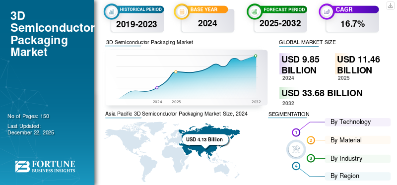
The global 3D semiconductor packaging market size was valued at USD 11.46 billion in 2025. The market is projected to grow from USD 13.34 billion in 2026 to USD 41.69 billion by 2034, exhibiting a CAGR of 15.31% during the forecast period. The Asia Pacific dominated the global market, accounting for a 42.27% share in 2025.
The market includes developing and distributing advanced packaging technology that integrates multiple semiconductor components to improve device performance and reduce size. This market is driven by the rising demand for compact, high-speed, and energy-efficient electronic devices across consumer electronics, automotive & transportation, IT & telecommunication, healthcare, industrial, aerospace & defense, and others. It incorporates through-silicon via, package-on-package, fan-out wafer-level packaging, wire bonded, system-in-package, and other technologies to develop advanced solutions.
Taiwan Semiconductor Manufacturing Company, Samsung Electronics, Intel Corporation, Advanced Semiconductor Engineering Group, Amkor Technology, JCET Group, United Microelectronics Corporation, Advanced Micro Devices, Inc., TEKTRONIX, INC., and Zeiss are the key companies operating in the market. These companies invest in research and development for improved performance, reduce costs, and meet the growing demands of high-performance computing and miniaturized devices. For instance,
- In September 2023, Intel introduced a glass substrate for next-gen advanced packaging. This innovation aims to support the transistor’s scaling and advance Moore’s Law for data-centric applications.
Download Free sample to learn more about this report.
IMPACT OF RECIPROCAL TARIFFS
Reciprocal tariffs between major economies can considerably impact the market by disrupting global supply chains and increasing production costs. The raw materials obtained globally can lead to higher manufacturing costs, slowing innovation and investment in this technology. For instance,
- The imposition of a 25% tariff on semiconductors by the U.S. is projected to have a significant influence on the global semiconductor industry. This policy measure will likely affect international trade dynamics, supply chain operations, and overall market competitiveness.
Additionally, reciprocal tariffs may help countries to localize the manufacturing of packaging operations to reduce dependency on imported suppliers. Although this could boost regional investments, it may lead to inefficiencies and increased competition for skilled labor. Therefore, the imposition of tariffs presents unpredictability in the market, affecting short and long-term strategic planning.
3D SEMICONDUCTOR PACKAGING MARKET TRENDS
Advancements in Through-Silicon Via (TSV) Technology Drive Market Growth
Constant advancements in TSV technology are contributing to the growth of the market. It offers a reliable method for producing high-density vertical connections between stacked chips, enhancing data transfer speed and energy efficiency. The growing need for miniaturized and high-performance devices further increases the need for compact and efficient system designs. For instance,
- Industry experts project significant growth in the miniaturized electronics market, with its value expected to rise from USD 47.25 billion in 2024 to USD 52.06 billion in 2025.
Moreover, these techniques reduce costs and improve manufacturing yields, making the technology more accessible for mass production. These developments drive adoption across various industries, including consumer electronics, IT & telecommunications, and automotive. Therefore, this technology supports the advanced 3D semiconductor packaging market growth.
MARKET DYNAMICS
Market Drivers
Growing Demand for Compact and High-Performance Devices Drives Market Expansion
The increasing demand for compact and high-performance electronic devices is a key market driver. The evolution of consumer electronics, IoT devices, and automotive systems increases the need for smaller form factors without compromising processing power or energy efficiency. For instance,
- According to IoT Analytics GmbH's State of IoT Summer 2024 report, IoT devices reached 16.6 billion by 2023, representing a 15% increase compared to 2022.
Traditional two-dimensional packaging technologies face limitations in meeting these requirements, creating opportunities for advanced 3D semiconductor packaging solutions.
3D semiconductor packaging enables vertical stacking of multiple chips, reducing device size while increasing performance. This capability is critical for smartphones, wearables, and high-performance computing applications where space and power efficiency are the major factors. Thus, the rising computational demand for miniaturization is accelerating the adoption of 3D packaging technologies across various industries.
Market Restraints
High Manufacturing Costs and Technical Challenges Restrain Market Growth
High manufacturing costs act as a major restraint in the market's growth. The production of 3D packages involves complex processes such as wafer thinning, Through-Silicon Via (TSV) formation, and precise arrangement, significantly increasing operating costs. These high costs limit adoption among small and medium enterprises in price-sensitive markets.
Moreover, technical challenges further hinder market growth. Issues such as thermal management, interconnect reliability, and testing complexity arise from the dense stacking of multiple dies within a package. It includes increasing development time, requiring advanced engineering expertise, and elevating the risk of yield loss, which restrains the adoption.
Market Opportunities
Artificial Intelligence (AI) and Machine Learning Expansion Unlocks New Growth Opportunities
The rapid expansion of AI and machine learning applications creates significant opportunities for the market. For instance,
- Industry specialists predict that the AI industry will experience a fivefold increase in value over the next five years.
AI systems require highly efficient, compact, and high-performance semiconductor components capable of processing large data capacities at high speeds. 3D packaging technology enables the vertical integration of multiple dies, improving data transfer rates and reducing latency.
Furthermore, healthcare, automotive, and telecommunications industries increasingly adopt AI-driven solutions, which demand advanced semiconductor packages. This trend boosts semiconductor manufacturers to invest in innovative 3D packaging techniques supporting the complex architectures required for AI and machine learning. Therefore, the growth of AI applications is expected to expand the 3D semiconductor packaging market share.
SEGMENTATION ANALYSIS
By Technology
Through-Silicon Via (TSV) Dominates Due to High-Density Vertical Interconnections and Superior Electrical Performance
Based on technology, the market is divided into Through-Silicon Via (TSV), Package-on-Package (PoP), Fan-out Wafer-Level Packaging, wire bonded, System-in-Package (SiP), and others.
Through-Silicon Via (TSV) dominates the market because it provides high-density vertical interconnections that significantly improve electrical performance and reduce signal delay with a share of 33.67%in 2026. TSV technology supports advanced applications requiring high bandwidth and low power consumption, making it essential for high-performance computing and data centers. Its mature fabrication processes and proven reliability contribute to its widespread adoption.
Package-on-Package (PoP) is expected to grow at the highest CAGR because it offers flexible, cost-effective integration of memory and logic components, particularly suited for mobile and consumer electronics with space constraints.
By Material
Organic Substrates Lead Owing to Cost-Effectiveness and Compatibility with High-Volume Manufacturing
Based on material, the market is divided into organic substrates, bonding wires, lead frames, encapsulation resins, ceramic packages, die attach materials, and others.
Organic substrates dominate the market with a share of 35.28% in 2026 owing to their cost-effectiveness and compatibility with high-volume manufacturing processes. They are also expected to grow at the highest CAGR owing to the growing demand for miniaturized and lightweight.
Bonding wires hold the second highest CAGR due to their widespread use as a reliable and affordable interconnection method in packaging, particularly in less complex or low-cost semiconductor devices.
By Industry
To know how our report can help streamline your business, Speak to Analyst
Consumer Electronics Dominates Due to Demand for Smaller, Faster, and Energy-Efficient Devices
Based on industry, the market is classified into consumer electronics, automotive & transportation, IT & telecommunication, healthcare, industrial, aerospace & defense, and others.
Consumer electronics dominate the market with a share of 29.86% in 2026, driven by the constant demand for smaller, faster, and more energy-efficient devices such as smartphones, tablets, and wearables. Rapid technological advancements and high consumer spending in this industry fuel the adoption of advanced packaging solutions.
The automotive & transportation industry is expected to grow at the highest CAGR due to the increasing integration of electronics in vehicles, including advanced driver assistance systems ADAS, EVs, and infotainment systems. Growing safety regulations and the shift toward autonomous driving technologies are accelerating demand for robust 3D semiconductor packages.
3D SEMICONDUCTOR PACKAGING MARKET REGIONAL OUTLOOK
North America
Asia Pacific 3D Semiconductor Packaging Market Size, 2025 (USD Billion)
To get more information on the regional analysis of this market, Download Free sample
In 2025, the North America market stood at USD 3.44 billion, representing 30.01% of global demand, and is projected to grow to USD 4.01 billion in 2026. North America holds the second-largest share of the market owing to its focus on high-performance computing, data centers, and cloud computing applications, which endures robust demand for advanced packaging technologies. Additionally, ongoing R&D investments and strategic collaborations further strengthen its position in the market. For instance,The U.S. market is projected to reach USD 1.41 billion by 2026.
- In November 2023, Amkor Technology, Inc. announced plans to establish an advanced packaging and test facility in Arizona. The company expects to invest approximately USD 2 billion and create around 2,000 jobs at the site.
The U.S. maintains a leading position in the market, driven by substantial government incentives under the CHIPS Act and strategic investments by major industry players in domestic advanced packaging facilities.
Asia Pacific
Download Free sample to learn more about this report.
Asia Pacific maintained a strong presence in the global market, reaching USD 4.84 billion in 2025, accounting for 42.27% share, and is expected to reach USD 5.68 billion in 2026. Asia Pacific dominates the market due to its established electronics manufacturing base and the presence of major players in China, South Korea, Taiwan, and Japan. For instance,
- In February 2023, United Microelectronics Corporation and Cadence Design Systems certified the Cadence 3D-IC reference flow for UMC’s chip stacking technologies. This certification aims to accelerate the time to market for advanced semiconductor designs.
It is also expected to grow at the highest CAGR owing to the increasing demand for advanced semiconductor solutions in consumer electronics, automotive, and industrial applications.The Japan market is projected to reach USD 1.32 billion by 2026, the China market is projected to reach USD 1.65 billion by 2026, and the India market is projected to reach USD 1.08 billion by 2026.
To know how our report can help streamline your business, Speak to Analyst
China dominates the Asia Pacific market due to its vast electronics manufacturing ecosystem, strong government support, and significant investments in semiconductor infrastructure. The presence of major assembly facilities and a strong demand for consumer electronics aids regional growth.
Europe
The Europe region captured 17.22% of the global market in 2025, generating USD 1.97 billion in revenue, and is projected to reach USD 2.28 billion in 2026. Europe maintains a significant market share due to its strong automotive industry and growing emphasis on industrial automation and smart manufacturing. Germany and the U.K. are investing in semiconductor innovation to reduce reliance on imports and enhance supply chain resilience. Furthermore, regional initiatives and funding promote the adoption of advanced packaging technologies across the region.The UK market is projected to reach USD 0.56 billion by 2026, while the Germany market is projected to reach USD 0.48 billion by 2026.
Middle East & Africa and South America
The Middle East & Africa market accounted for USD 0.56 billion in 2025, representing 4.89% of the global industry, and is expected to reach USD 0.64 billion in 2026. South America and the Middle East & Africa are expected to grow more slowly due to limited domestic semiconductor production capabilities and infrastructure. Economic constraints, political instability, and lower R&D investment restrict the development and adoption of advanced packaging technologies. Thus, these regions exhibit slower market expansion.
COMPETITIVE LANDSCAPE
KEY INDUSTRY PLAYERS
Key Players Launch New Products to Strengthen Market Positioning
Players launch new product portfolios to enhance their market position by leveraging technological advancements, addressing diverse consumer needs, and staying ahead of competitors. They prioritize portfolio enhancement and strategic collaborations, acquisitions, and partnerships to strengthen their product offerings. Such strategic product launches help companies maintain and grow their market share in a rapidly evolving industry.
Long List of Companies Studied (including but not limited to)
- Taiwan Semiconductor Manufacturing Company (Taiwan)
- Samsung Electronics (South Korea)
- Intel Corporation (U.S.)
- Advanced Semiconductor Engineering Group (Taiwan)
- Amkor Technology (U.S.)
- JCET Group (China)
- United Microelectronics Corporation (Taiwan)
- Advanced Micro Devices, Inc. (U.S.)
- TEKTRONIX, INC. (U.S.)
- Zeiss (Germany)
- Qualcomm Technologies Inc. (U.S.)
- STMicroelectronics (Switzerland)
- Broadcom Inc. (U.S.)
- IBM Corporation (U.S.)
- Sony Corporation (Japan)
- Texas Instruments (U.S.)
- Xilinx Inc. (U.S.)
- SUSS MicroTec (Germany)
- BE Semiconductor Industries N.V. (Netherlands)
And more..
KEY INDUSTRY DEVELOPMENTS
- In April 2025, Siemens and Intel achieved multiple product certifications and enhanced reference flows for next-gen ICs and advanced packaging.
- In March 2025, Kyocera showcased its ceramic and single-crystal sapphire engineering solutions at Pittcon. It is a globally recognized event for analytical, laboratory, and life science equipment and solutions.
- In February 2025, Advanced Semiconductor Engineering, Inc. inaugurated its fifth manufacturing facility in Malaysia. The new plant is expected to enhance production capacity for advanced packaging technologies, aligning with growing demand for next-gen applications such as GenAI.
- In October 2024, Calumet Electronics and KLA Corporation developed organic substrate technology in the U.S. This development supports advanced semiconductor packaging for aerospace, high-performance computing, and AI applications.
- In October 2024, Amkor Technology, Inc. and TSMC signed a memorandum of understanding to develop advanced packaging jointly. This collaboration aims to strengthen and expand the region’s semiconductor ecosystem.
REPORT COVERAGE
The market report focuses on key aspects such as leading companies and product/service types. Besides, the report offers insights into the market trend analysis and highlights vital industry developments. In addition to the factors above, the report encompasses several factors that contributed to the market's growth in recent years.
Request for Customization to gain extensive market insights.
REPORT SCOPE & SEGMENTATION
|
ATTRIBUTE |
DETAILS |
|
|
Study Period |
2021-2034 |
|
|
Base Year |
2025 |
|
|
Estimated Year |
2026 |
|
|
Forecast Period |
2026-2034 |
|
|
Historical Period |
2021-2024 |
|
|
Unit |
Value (USD Billion) |
|
|
Growth Rate |
CAGR of 15.31% from 2026 to 2034 |
|
|
Segmentation |
By Technology
By Material
By Industry
By Region
|
|
|
Companies Profiled in the Report |
· Taiwan Semiconductor Manufacturing Company (Taiwan) · Samsung Electronics (South Korea) · Intel Corporation (U.S.) · Advanced Semiconductor Engineering Group (Taiwan) · Amkor Technology (U.S.) · JCET Group (China) · United Microelectronics Corporation (Taiwan) · Advanced Micro Devices, Inc. (U.S.) · TEKTRONIX, INC. (U.S.) · Zeiss (Germany) |
|
Frequently Asked Questions
The market is projected to reach USD 41.69 billion by 2034.
In 2025, the market size stood at USD 11.46 billion.
The market is projected to grow at a CAGR of 15.31% during the forecast period.
The consumer electronics sector is leading the market.
Growing demand for compact and high-performance devices drives the expansion of the 3D semiconductor packaging market.
Taiwan Semiconductor Manufacturing Company, Samsung Electronics, Intel Corporation, and Advanced Semiconductor Engineering Group are the top players in the market.
Asia Pacific holds the highest market share.
Asia Pacific is expected to grow with the highest CAGR during the forecast period.


- 2021-2034
- 2025
- 2021-2024
- 150
Get 30-60 hrs Free Customization
Expand Regional and Country Coverage, Segments Analysis, Company Profiles, Competitive Benchmarking, and End-user Insights.
Related Reports
-
US +1 833 909 2966 ( Toll Free )
-
Get In Touch With Us