EUV Lithography Market Size, Share & Industry Analysis, By Equipment (Light Source, Optics, Mask, and Others), By End-user (Integrated Device Manufacturer and Foundries), and Regional Forecast, 2026-2034
KEY MARKET INSIGHTS
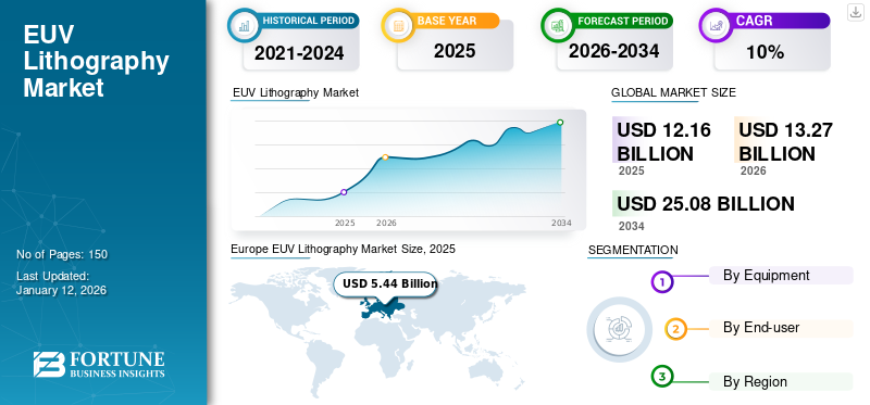
The global EUV lithography market size was valued at USD 12.16 billion in 2025. The market is projected to grow from USD 13.27 billion in 2026 to USD 25.08 billion by 2034, exhibiting a CAGR of 8.28% during the forecast period. Europe dominated the market with a share of 44.71% in 2025.
EUV light, also known as extreme ultraviolet light designed for microchip lithography, covers a microprocessor wafer in a photosensitive material and cautiously exposes it to light. This designs a pattern on the wafer, which is used for further steps in the microchip design process. It allows the production of chips through structures less than 7 nanometers, pushing the limitations of Moore’s law. This rule has accelerated the growth of computing power by expanding the number of transistors on a microchip about every two years.
The global market is poised for significant growth, driven by the increasing product demand in data centers, consumer electronics, and scalability in several applications. Key players in the market include ASML (Netherlands), Samsung Electronics Co. Ltd. (South Korea), and KLA Corporation (U.S.), with products, such as TWINSCAN EXE:5000 and Samsung 7LPP modules. The market's future will likely witness technological innovations concentrated on augmenting durability and efficiency in extreme conditions.
The COVID-19 pandemic significantly impacted the market. Despite the high demand, the pandemic-related safety protocols and restrictions on semiconductor fabrication, particularly in Asia, led to a manufacturing slowdown in some cases. Although major semiconductor companies adapted by implementing new safety protocols, there were delays in the implementation and calibration of new machines, which required highly skilled personnel. These delays, combined with component shortages, created bottlenecks in the product’s production and installation.
Download Free sample to learn more about this report.
IMPACT OF GENERATIVE AI
Increased Adoption of Generative AI in Manufacturing Processes to Boost Market Growth
Generative AI significantly impacts the market due to advancements in process optimization, defect detection, and design automation. EUV lithography is crucial for the semiconductor industry, allowing manufacturers to create smaller and more complex chips. These AI models aid in optimizing lithography patterns and simulation models, improving the precision and speed of EUV processes. By analyzing large datasets from previous manufacturing runs, generative AI can generate optimized patterns that minimize defects, improve yield, and reduce trial-and-error in manufacturing processes. Hence, these factors will boost the global EUV lithography market growth.
MARKET DYNAMICS
Market Drivers
Rising Complexity of Integrated Circuits in Semiconductor Devices to Drive Product Demand
As Integrated Circuits (ICs) are becoming more complex in nature, there is an increasing need for semiconductor equipment with more complex and innovative designs. As ICs become more progressive, they need detailed lithography procedures to attain the anticipated functionality and performance. This complication is driven by various factors, such as need for smaller feature sizes, demand for better transistor density, and incorporation of architectures of new devices. EUV lithography acts as an essential driver for the market as it allows the construction of these complicated ICs. EUV lithography technology employs high-intensity UV light that has a smaller wavelength to make minor and more complex designs on chip wafers. Since EUV lithography has a higher resolution and better control over some key dimensions, it encourages chip manufacturers to attain the accuracy and precision essential for cutting-edge integrated circuit designs. These factors will drive the growth of the market.
Market Restraints
Higher Cost of Implementing EUV Lithography System May Hamper Market Growth
The higher cost related to executing EUV lithography is an important restraining factor. The technology necessitates the use of exclusive and multifaceted equipment, such as EUV masks, light sources, and photoresists. The existing price of EUV machines is several times higher than that of outdated optical lithography tools. This price factor creates an obstacle for smaller semiconductor producers or foundries that may not have the economic resources to implement the EUV lithography technology. This technology also necessitates the use of certain complex equipment, which contributes to higher implementation costs. Key components of this technology include EUV light sources, masks, photoresists, and scanners. These components are expensive to manufacture, develop, and maintain.
Moreover, technical challenges, such as the necessity for robust pellicles to protect photomasks and the hurdle of scaling laboratory techniques to industrial production, complicate its adoption. However, as these concerns are addressed, EUV lithography is becoming essential for generating memory devices and advanced processors that power modern electronics.
Market Opportunities
Rise in Deployment of Data Centers to Boost Product Demand
The development of EUV lithography in manufacturing offers a significant opportunity for the market. Memory devices, such as NAND Flash and DRAM play a vital role in several electronic devices, including smartphones, computers, and data centers. As memory technology progresses, there is an increasing demand for advanced capacity, quicker, and energy-efficient memory solutions. EUV lithography provides unique advantages that make it an attractive choice for the production of innovative memory devices. Thus, by using EUV lithography, memory producers can overcome the restrictions of traditional optical lithography, which struggles to accomplish the necessary pattern resolution and reliability for progressive memory designs.
EUV LITHOGRAPHY MARKET TRENDS
Rising Demand for Advanced Semiconductor Nodes in Several Chips to Drive Market Progress
The growth of the market is significantly driven by the increasing demand for innovative semiconductor nodes, mainly in the production of 5nm-and-below chips. As tech leaders, including Samsung and TSMC, upgrade their manufacturing abilities for creating cutting-edge processors, EUV lithography has become crucial for attaining the high resolution needed for these nodes. For instance,
- TSMC partnered with ASML to increase its EUV capacity, highlighting this trend and ensuring that they meet the rising requirements of applications, including artificial intelligence and 5G technology.
This growing focus on miniaturization and performance is a key factor driving the market.
Download Free sample to learn more about this report.
SEGMENTATION ANALYSIS
By Equipment Type
Adoption of Light Source Equipment Increased Among Semiconductor Device Producers to Manufacture Smaller Chips
On the basis of equipment type, the market is categorized into light source, optics, mask, and others.
The diagnostics segment is projected to dominate the market with a share of 41.26% in 2026. The segment is growing at a substantial rate as the semiconductor sector pushes the production of smaller, more effective chips. This demand is attributed to the key role played by EUV lithography in enabling creation of patterned sub-10 nanometer topographies on silicon-based wafers, which is important for next-gen semiconductor equipment. Rising innovations in light source technology, significant investments from prominent producers of semiconductor chips, collaborations between manufacturers to facilitate technological developments, and rising support from governments to conduct large-scale semiconductor R&D are the main factors driving the segment’s growth.
The mask segment is expected to record the highest CAGR during the forecast period due to the high demand for innovative semiconductor devices. Since EUV lithography is facilitating the production of semiconductors that are sized at sub-7 nanometers, the precision and complexity in the creation of masks have increased considerably. Masks or photomasks play a vital role in transferring the circuit outlines onto chip wafers, and the accuracy of this process has a direct impact on the yield and performance of the final product.
To know how our report can help streamline your business, Speak to Analyst
By End-user
Rising Demand for Advanced Electronic Devices Fueled Product Adoption Among Integrated Device Manufacturers
Based on end-user, the market is categorized into integrated device manufacturer and foundries.
The Integrated Device Manufacturer (IDM) segment holds the largest global EUV lithography market share in 2024. IDM corporations, which are involved in the manufacture, design, and sales of semiconductor products, are progressively implementing EUV lithography to overcome the limitations of chip Power, Performance, and Area (PPA). This implementation is driven by the increasing demand for more advanced electronic devices across various applications, such as mobile, computing, IoT, and automotive. Furthermore, EUV lithography, with its ability to pattern extremely fine structures on silicon wafers, is critical to generating next-generation semiconductor devices. The segment is set to be capture 53.92% of the market share in 2026.
The foundries segment is expected to record the highest CAGR of 12.27% during the forecast period due to their critical role in transforming the production of semiconductors. As the business of chipmaking endures its insistent drive toward lesser, more dominant, and energy-saving procedures, foundries are progressively becoming reliant on the extreme ultraviolet lithography technology to cater to these complex technical requirements. The EUV lithography technology, which is well-known for creating extremely detailed features on silicon-based wafers, is crucial for manufacturing the advanced semiconductors that are needed for several applications, such as artificial intelligence, smartphones, high-performance computing, and automotive.
EUV LITHOGRAPHY MARKET REGIONAL OUTLOOK
Europe
Europe EUV Lithography Market Size, 2025 (USD Billion)
To get more information on the regional analysis of this market, Download Free sample
In 2025, Europe generated USD 5.44 billion, contributing 44.71% to the global market revenue, and is projected to grow to USD 6.02 billion in 2026. The market is driven by developments in semiconductor technology and a robust research and development ecosystem. The U.K. market is expanding, expected to hit USD 1.09 billion in 2026. European semiconductor producers and research institutions are leveraging EUV lithography to push the limitations of chip reduction and routine keys to adapt to the rapidly developing tech landscape. For instance,
- October 2023: Intel launched two new chip fabs in Germany. Intel and the German government invested about USD 30 billion to build two cutting-edge semiconductor plants in Germany. This investment includes a USD 4.6 billion chip plant in Poland and a USD 25 billion factory in Israel, thereby designing a series of substantial investments in the semiconductor industry.
Moreover, the constant development and introduction of innovative technologies are the main factors driving the German EUV lithography market. The enhanced competencies, improved efficacy, and innovative product features attract more customers and companies to accept these solutions. Germany is set to be valued at USD 1.39 billion in 2026. France is projected to reach a market value of USD 1.11 billion in 2025.
North America
North America maintained a strong presence in the global market, reaching USD 1.8 billion in 2025, accounting for 14.80% share, and is expected to reach USD 1.89 billion in 2026. The region witnessed significant growth in the global market, supported by the increasing demand for smaller, more dominant semiconductor devices across a range of industries, including telecommunications, computing, and consumer electronics. As the pursuit for reduction continues, with semiconductor companies pushing the limitations of Moore's Law, EUV lithography has emerged as a critical technology enabling the making of chips through feature sizes well under 10 nanometres. This is driving the development of the market in the region. The U.S. market is estimated to acquire USD 1.18 billion in 2026.
Asia Pacific
The Asia Pacific market accounted for USD 3.4 billion in 2025, representing 27.96% of the global industry, and is expected to reach USD 3.73 billion in 2026. The region is witnessing the highest CAGR of 12.34% during the forecast period, due to its strong semiconductor manufacturing base and the presence of leading semiconductor foundries. China is expected to hold USD 1.03 billion in 2025. Taiwan, South Korea, and China have some of the world's largest semiconductor manufacturing firms and foundries, including TSMC, Samsung, and SMIC. These companies are at the forefront of executing cutting-edge manufacturing technologies, including EUV lithography, which will drive the regional market’s growth. India is estimated to gain USD 0.50 billion in 2026. France is likely to reach USD 0.95 billion in 2025.
Middle East & Africa (MEA) and South America
In 2025, Middle East & Africa represented USD 0.9 billion, accounting for 7.38% of the worldwide market, and is projected to grow to USD 0.96 billion in 2026. The markets in the Middle East & Africa and South America are still emerging but showing major potential. Many countries in the MEA region have made substantial investments in expanding their semiconductor manufacturing abilities. Therefore, with the adoption of EUV lithography technology in the region, consistent investments have fueled the growth of local semiconductor industries in MEA.
Similarly, the market in South America is expected to grow at a moderate rate. Governments worldwide are significantly investing in research and development, supporting the development of EUV lithography. However, the market's growth may be hindered by economic challenges and incomplete technological infrastructure in the region. The GCC market is likely to attain USD 0.29 billion in 2025.
Latin America
Latin America contributed 5.15% to the global market in 2025, with a valuation of USD 0.63 billion, and is projected to reach USD 0.67 billion in 2026.
COMPETITIVE LANDSCAPE
Key Industry Players
Effective Strategies and Development of Advanced Products to Aid in Market Development
Numerous renowned companies are developing cutting-edge products to increase their market presence globally. To cement their position as a leading EUV lithography provider, these companies are partnering with both local and international firms along with acquisitions. In addition to the above strategies, there is a keen focus on implementing effective plans to garner a significant share of the market. The amplified demand of EUV lithography in many sectors plays a key role in creating a positive outlook for the market.
List of Key EUV Lithography Companies Profiled:
- ASML (Netherlands)
- Samsung Electronics Co. Ltd. (South Korea)
- Canon Inc. (Japan)
- KLA Corporation (U.S.)
- NTT Advanced Technology Corporation (Japan)
- Nikon Corporation (China)
- ZEISS Group (Germany)
- ADVANTEST CORPORATION (Japan)
- SUSS MicroTec SE (Germany)
- AGC Inc. (Japan)
- Ushio Inc. (Japan)
- Energetiq Technology Inc. (U.S.)
- Photronics, Inc. (U.S.)
- Toppan Photomasks (Japan)
- Rigaku Corporation (Japan)
- Zygo Corporation (U.S.)
KEY INDUSTRY DEVELOPMENTS:
- August 2024: Amphenol Corporation acquired the Carlisle Interconnect Technologies (CIT) business from Carlisle. The acquisition improved Amphenol’s product portfolio for massively engineered severe environment interconnect solutions. This move is expected to help the company offer a more complete technology posing for its clients in the commercial air, defense, and industrial markets.
- August 2024: Imec established logic and DRAM structures with High NA EUV lithography. The launch organized dedicated wafer stacks and relocated High NA EUV baseline procedures to the 0.55NA EUV scanner.
- June 2024: ASML and Imec launched a high NA EUV Lithography lab for enabling faster adoption in mass manufacturing. The launch delivered a wider ecosystem of equipment and material suppliers with a High NA patterning program and handling meteorology tools.
- October 2023: Canon Inc. introduced the FPA-1200NZ2C, an equipment proficient in manufacturing semiconductors that use Nanoimprint Lithography (NIL). The technology aided in printing the proposal of a chip circuit onto a semiconductor wafer.
- February 2023: Applied Materials Inc. launched an advanced designing technology that permits chipmakers to generate high-performance transistors and interrelate wiring through fewer EUV lithography steps. This will reduce the cost, difficulty, and environmental impact of innovative chipmaking.
INVESTMENT ANALYSIS AND OPPORTUNITIES
The market is focused on research & development activities to develop more advanced, efficient, and cost-effective solutions. Companies are increasingly collaborating with small organizations, providing opportunities for mergers and acquisitions. The market is highly consolidated as ASML is the only producer of lithography machines that uses extreme ultraviolet light. The organization manufactures and sells its tools to global semiconductor fabricators, such as Intel, Samsung, and Taiwan Semiconductor Manufacturing Company (TSMC). Nearly 25% of the organization’s revenues are derived from the sales of EUV lithography systems, which reinforces its monopoly in the commercialization of industrial EUV lithography systems.
REPORT COVERAGE
The report provides a detailed analysis of the market and focuses on key aspects, such as leading companies, product types, and leading applications of the product. Besides, it offers insights into the market trends and highlights key industry developments. In addition to the factors mentioned above, the report encompasses several factors that have contributed to the growth of the market in recent years.
Request for Customization to gain extensive market insights.
REPORT SCOPE & SEGMENTATION
|
ATTRIBUTE |
DETAILS |
|
Study Period |
2021-2034 |
|
Base Year |
2025 |
|
Estimated Year |
2026 |
|
Forecast Period |
2026-2034 |
|
Historical Period |
2021-2024 |
|
Growth Rate |
CAGR of 8.28% from 2026 to 2034 |
|
Unit |
Value (USD Billion) |
|
Segmentation |
By Equipment, End-user, and Region |
|
Segmentation |
By Equipment
By End-user
By Region
|
|
Companies Profiled in the Report |
ASML (Netherlands), Samsung Electronics Co. Ltd. (South Korea), Canon Inc. (Japan), KLA Corporation (U.S.), NTT Advanced Technology Corporation (Japan), Nikon Corporation (China), ZEISS Group (Germany), ADVANTEST CORPORATION (Japan), SUSS MicroTec SE (Germany) |
Frequently Asked Questions
The market value is projected to reach USD 25.08 billion by 2034.
In 2025, the market is valued at USD 12.16 billion.
The market is projected to register a CAGR of 8.28% during the forecast period.
The light source equipment segment is expected to lead the market.
Increasing complexity of integrated circuits in semiconductor devices is the key factor driving the markets growth.
ASML, Samsung Groups Co. Ltd., Canon Inc., NTT Advanced Technology Corporation, Nikon Corporation, KLA Corporation, ADVANTEST CORPORATION, Ushio Inc., TOPPAN PHOTOMASKS, and SUSS MicroTec SE are the top players in the market.
Europe is expected to hold the highest market share.
By end-user, the foundries segment is expected to record the highest CAGR during the forecast period.


- 2021-2034
- 2025
- 2021-2024
- 150
Get 20% Free Customization
Expand Regional and Country Coverage, Segments Analysis, Company Profiles, Competitive Benchmarking, and End-user Insights.
Related Reports
-
US +1 833 909 2966 ( Toll Free )
-
Get In Touch With Us