Wire Bonder Equipment Market Size, Share & Industry Analysis, By Type (Ball Bonders, Wedge Bonders, Stud-Bump Bonders, and Others), By Bonding Technology (Thermosonic Bonding, Ultrasonic Bonding, Thermocompression Bonding, and Others), By Automation (Fully Automatic, Semi-Automatic, and Manual), By End User (Integrated Device Manufacturers (IDMs) and Outsourced Semiconductor Assembly, and Testing (OSATs)), and Regional Forecast, 2026 – 2034
 Download Free Sample

Wire Bonder Equipment Market Size and Future Outlook
 Listen to Audio Version
The wire bonder equipment market size was valued at USD 1,095.0 million in 2025. The market is projected to grow from USD 1,186.2 million in 2026 to USD 2,140.9 million by 2034, exhibiting a CAGR of 7.7% during the forecast period.
The market comprises manufacturing and commercial sale of semiconductor packaging equipment used to create electrical interconnections between semiconductor dies and package terminals through fine and heavy metallic wires. These wire bonding machines enable precise bond formation by controlling placement accuracy, bond force, ultrasonic energy, loop geometry, throughput, and process stability across semiconductor assembly operations. Wire bonding equipment supports integrated circuit packaging, memory devices, logic and analog ICs, power semiconductors, automotive electronics, MEMS and sensors, LEDs, and other microelectronics assembly applications. Increasing package miniaturization, higher interconnect density, expanding power semiconductor production, and advanced packaging requirements are encouraging manufacturers to enhance bonding speed, placement precision, wire-loop control, vision alignment, and real-time process monitoring. Equipment suppliers are consequently advancing copper wire bonding, aluminum wire bonding, gold wire bonding, automated recipe optimization, intelligent inspection, higher-force wedge bonding, fine-wire handling, and integrated production-data capabilities to improve yield and extend wire bonding applications across next-generation chip packaging and electronic component assembly requirements.
- For instance, in March 2026, Kulicke & Soffa introduced its ProMEM suite of memory-focused ball-bonding enhancements, combining improvements across first bond, second bond, bumping, and looping processes to deliver up to 20% higher throughput while supporting higher-density DRAM and NAND packaging architectures.
Kulicke & Soffa Industries, Inc., ASMPT Limited, Besi N.V., Hesse GmbH, and F&K Delvotec Bondtechnik GmbH are among the major companies operating in the global market.
WIRE BONDER EQUIPMENT MARKET TRENDS
Shift toward Advanced Transducer Architectures and Adaptive Process Automation is Redefining Wire Bonding Performance
The market is shifting toward advanced wire bonding technologies and adaptive process automation as semiconductor manufacturers seek improved process stability, higher yield, and consistent production performance without compromising throughput. Conventional bonding platforms are increasingly being enhanced with redesigned ultrasonic subsystems that reduce mechanical limitations, improve energy transfer efficiency, and enable more precise bond formation. Equipment suppliers are integrating lightweight composite transducers, digitally controlled ultrasonic generators, automated parameter adjustment, and software-driven process optimization to support increasingly complex semiconductor packaging requirements. This evolution is particularly important for high-density integrated circuit packaging, where variations in substrate characteristics, metallization quality, package design, and bonding parameters can influence production consistency. Next-generation wire bonding machines are also incorporating automated setup capabilities, intelligent monitoring, and advanced control systems to reduce operator dependency and accelerate transitions between device configurations. Consequently, semiconductor manufacturing equipment providers are moving beyond basic speed enhancements toward adaptive platforms that combine mechanical innovation, process intelligence, and automation to support advanced microelectronics assembly and increasingly complex chip packaging applications.
- For instance, in April 2025, ASMPT introduced enhanced features for its AERO PRO XPOWER 2.0 wire bonder, integrating upgraded hardware and software for improved bonding precision alongside smart process automation designed to adapt bonding operations to changing production requirements.
MARKET DYNAMICS
MARKET DRIVERS
Download Free sample to learn more about this report.
Gradual Shift From Gold Toward Copper-Based Interconnects in High-Volume Semiconductor Assembly Boosts Market Growth
The wire bonder equipment market growth is being supported by the established migration from gold toward copper-based interconnects in high-volume semiconductor assembly. Copper offers lower material cost and favorable electrical and thermal characteristics, making it attractive for cost-sensitive logic, analog, discrete, and other high-volume packages. However, copper bonding requires tightly controlled free-air-ball formation, bond force, ultrasonic conditions, capillary design, protective atmosphere, and looping parameters, encouraging semiconductor assemblers to deploy bonders equipped with dedicated copper-process capabilities. This creates demand not merely from increasing semiconductor output but from the need to maintain high yield while processing harder wire materials without damaging sensitive bond pads. Equipment suppliers are consequently commercializing mature copper-specific process libraries and hardware configurations, enabling manufacturers to lower interconnect material expenditure while retaining production consistency at scale.
- For instance, in November 2025, Kulicke & Soffa stated in its fiscal 2025 filing that collaboration with customers and material suppliers had made copper wire bonding widely accepted and had significantly reduced integrated-circuit assembly costs.
Market Drivers - Impact & CAGR Contribution (2026–2034)
| Rank | Market Drivers | Expected Impact on Market Growth | Estimated Gross Market Growth Contribution (USD Million) | Impact: 2026-2028 | Impact: 2029-2031 | Impact: 2032-2034 |
|---|---|---|---|---|---|---|
| 1 | Rapid Expansion of AI Data Centers and High-Performance Computing Infrastructure | High | 330.0 | High | High | High |
| 2 | Increasing Adoption of Advanced Semiconductor Packaging for Automotive, Power Electronics, and Memory Applications | High | 220.0 | Medium-High | High | High |
| 3 | Cost advantages of copper wire bonding to sustain demand for advanced ball bonder platforms | Medium-High | 180.0 | Medium | High | High |
| 4 | Expansion of OSAT Capacity and Semiconductor Manufacturing Localization Initiatives | Medium-High | 150.0 | Medium | High | Medium-High |
| 5 | Rising Adoption of Automated Wire Bonding Platforms and Smart Manufacturing Integration | Medium | 120.0 | Medium | Medium-High | High |
| 6 | Others, Including MEMS, Sensors, LED Packaging, Aerospace Electronics, and Specialty Semiconductor Applications | Medium-Low | 80.0 | Medium-Low | Medium | Medium-High |
| Total Gross Growth Contribution | 1,080 | |||||
Source: Fortune Business Insights
Download Free sample For In-Depth Market Restraints & Risk Analysis
MARKET RESTRAINTS
Strong Purchasing Leverage of Large IDMs and OSATs to Limit Equipment Pricing Expansion
The market faces restraint from concentrated purchasing power of major semiconductor manufacturers and outsourced assembly providers that acquire machines in substantial volumes. Large IDMs and OSATs can negotiate equipment pricing, configuration packages, service terms, acceptance conditions, and multi-machine procurement agreements more aggressively than smaller semiconductor assemblers. Wire bonders must also undergo customer-specific process qualification before broader deployment, particularly when a platform is introduced across multiple factories or package families. This procurement structure can constrain average selling-price expansion even when equipment capabilities improve materially. Suppliers must therefore balance customized machine configurations and application support against customer expectations for volume-based pricing. Competitive qualification involving multiple equipment vendors can further lengthen purchasing decisions, while approved legacy platforms may remain favored until a new system demonstrates clear throughput, yield, or cost-of-ownership advantages.
Market Restraints - Impact & Negative CAGR Contribution (2026–2034)
| Rank | Market Restraints | Expected Impact on Market Growth | Estimated Reduction in Market Size (USD Million) | Impact: 2026-2028 | Impact: 2029-2031 | Impact: 2032-2034 |
|---|---|---|---|---|---|---|
| 1 | Semiconductor Equipment Investment Cyclicality and Delayed Capital Expenditure Decisions | High | 45.0 | High | Medium-High | Medium |
| 2 | Strong purchasing leverage of large IDMS and OSATS to limit equipment pricing expansion | Medium-High | 32.0 | Medium | High | High |
| 3 | High Initial Equipment Cost and Lengthy Customer Qualification Cycles | Medium | 28.0 | High | Medium | Medium |
| 4 | Others, Including Supply Chain Constraints, Specialized Component Availability, and Technology Transition Risks | Medium-Low | 20.3 | Medium | Medium | Medium-Low |
| Total Market Reduction | 125.3 | |||||
Source: Fortune Business Insights
Download Free sample For In-Depth Market Restraints & Risk Analysis
MARKET OPPORTUNITIES
Expansion of SiC and GaN Power Semiconductor Production to Create Growth Opportunities
Growing manufacturing of silicon carbide and gallium nitride power devices is creating attractive opportunities for heavy-wire and ribbon bonding equipment used in high-current semiconductor modules. Power devices employed in electric vehicles, renewable-energy converters, industrial drives, charging infrastructure, rail systems, and data-center power supplies require interconnections capable of carrying substantial electrical loads while tolerating repeated thermal cycling. These requirements support continued use and development of ultrasonic wedge bonding with aluminum, copper, and ribbon interconnects across power-module assembly. Wider adoption of 200 mm SiC manufacturing is also expected to increase downstream packaging volumes, encouraging power-semiconductor producers and packaging partners to invest in scalable bonding capacity. Equipment suppliers can consequently address demand through larger working areas, multiple bondhead configurations, stronger force capability, advanced wire handling, and process monitoring tailored to power devices rather than conventional fine-wire IC packaging.
- For instance, in February 2025, Infineon announced the release of its first SiC products produced using 200 mm wafer technology and stated that its newly constructed Module 3 in Kulim, Malaysia, was positioned to commence high-volume production in line with market demand.
MARKET CHALLENGES
Growing Adoption of Flip-Chip, Thermocompression, and Hybrid Bonding to Challenge Wire Bonding in Leading-Edge Packages
Wire bonder equipment manufacturers face increasing competitive pressure from alternative interconnect technologies as leading-edge semiconductor packages require extremely short electrical paths, higher interconnect density, greater bandwidth, and increasingly complex three-dimensional integration. Flip-chip, micro-bump thermocompression bonding, and hybrid bonding are gaining importance in AI accelerators, advanced logic, high-bandwidth memory, and heterogeneous integration architectures where conventional wire loops may impose package-height or interconnect-density limitations. This does not eliminate wire bonding, which retains significant advantages in manufacturing maturity, flexibility, throughput, and cost across a broad range of semiconductor packages, but it can restrict its penetration in the highest-performance package classes. Wire-bonder suppliers must therefore continually extend fine-pitch capability, vertical interconnection approaches, loop control, material flexibility, and productivity to retain competitiveness as packaging architectures evolve.
Segmentation Analysis
By Type
Ball Bonders Segment Led Market Owing to Mature Process Ecosystem and Broad Package Compatibility
By type, the market is segmented into ball bonders, wedge bonders, stud-bump bonders, and others.
The ball bonders segment accounted for largest market share in 2025, supported by the technology’s mature manufacturing ecosystem, extensive installed base, and ability to support diverse semiconductor package formats with consistent production performance. Ball bonding platforms provide manufacturers with established process recipes, optimized tooling availability, and proven reliability across multiple package configurations, reducing qualification requirements while expanding or upgrading assembly capacity. The segment benefits from continuous improvements in capillary design, motion-control accuracy, bond-force management, and vision-assisted alignment, which enable equipment suppliers to improve yield while accommodating tighter pitch requirements and increasingly complex package layouts.
- For instance, in August 2025, ASMPT announced that it would showcase its AERO PRO fine-pitch wire bonder at SEMICON India, highlighting high-speed bonding of 0.5 mil wires, 22 µm bond balls, mixed-wire capability, and real-time process monitoring for high-density semiconductor packaging.
The wedge bonders segment is projected to register the highest CAGR of approximately 10.0% during the forecast period, supported by increasing requirements for flexible ultrasonic interconnection across matrix leadframes, RF/HF components, optoelectronics, hybrid assemblies, and specialized semiconductor packages.
To know how our report can help streamline your business, Speak to Analyst
By Bonding Technology
Thermosonic Bonding Segment Led the Market Owing to Established Integration Across Fine-Pitch Semiconductor Packaging Applications
By bonding technology, the market is segmented into thermosonic bonding, ultrasonic bonding, thermocompression bonding, and others.
The thermosonic bonding segment accounted for the largest wire bonder equipment market share in 2025, supported by its strong compatibility with fine-wire interconnection requirements, mature process control capabilities, and widespread acceptance among semiconductor packaging manufacturers. The technology combines controlled thermal energy with ultrasonic vibration to achieve reliable bonding at relatively low mechanical stress levels, making it suitable for delicate semiconductor structures where maintaining pad integrity and bond reliability is critical. Thermosonic platforms provide manufacturers with precise control over bonding parameters such as temperature, ultrasonic energy, force, and loop formation, enabling consistent performance across different package designs. The segment also benefits from continuous improvements in transducer systems, automated calibration, advanced vision alignment, and software-based process optimization that help manufacturers improve yield and reduce variation during production.
The ultrasonic bonding segment is projected to register the highest CAGR of approximately 10.7% during the forecast period, driven by increasing adoption in power semiconductor packaging, automotive electronics, and high-reliability electronic assemblies requiring robust solid-state interconnections.
By Automation
Fully Automatic Segment Dominated Owing to Higher Production Efficiency and Reduced Operator Dependency
By automation, the market is segmented into fully automatic, semi-automatic, and manual.
The fully automatic segment accounted for the largest market share in 2025, supported by its ability to deliver consistent bonding quality, high repeatability, and improved production efficiency across semiconductor manufacturing environments. Fully automatic wire bonders integrate automated wafer handling, die recognition, vision alignment, programmable bonding sequences, and real-time process monitoring, allowing manufacturers to maintain stable output across large production volumes. The segment is increasingly preferred by IDMs and OSATs seeking to minimize process variation, improve equipment utilization, and reduce dependency on manual adjustments during semiconductor assembly operations. Advanced automation features such as automatic recipe management, self-calibration, predictive maintenance capabilities, and factory-level data connectivity are further enhancing the value proposition of fully automated platforms.
The semi-automatic segment is projected to register a CAGR of approximately 3.3% during the forecast period, supported by continued demand from research laboratories, pilot production facilities, specialty semiconductor manufacturers, and applications requiring greater operator control during bonding operations.
By End User
High Equipment Utilization and Large-Scale Packaging Capacity Requirements Contributed to Outsourced Semiconductor Assembly and Testing (OSATs) Segment’s Dominance
By end user, the market is segmented into Integrated Device Manufacturers (IDMs) and Outsourced Semiconductor Assembly and Testing (OSATs).
The OSATs segment accounted for the largest market share in 2025, supported by extensive deployment of wire bonding equipment across large-scale third-party semiconductor packaging facilities serving multiple chip manufacturers. OSATs operate diverse assembly lines covering automotive semiconductors, consumer electronics components, memory devices, analog ICs, power semiconductors, and specialty packages, creating continuous requirements for flexible and high-throughput bonding platforms. Their business models require maintaining broad equipment capabilities to accommodate varying customer specifications, package formats, and production volumes within the same manufacturing infrastructure. Additionally, OSAT companies frequently invest in equipment upgrades and capacity additions to improve manufacturing flexibility, support new semiconductor technologies, and meet customer qualification requirements.
The Integrated Device Manufacturers (IDMs) segment is projected to register a CAGR of approximately 6.6% during the forecast period, supported by increasing internalization of semiconductor packaging activities, especially for automotive electronics, power devices, sensors, and specialized semiconductor products requiring tighter control over manufacturing processes.
Wire Bonder Equipment Market Regional Outlook
By geography, the market is categorized into Europe, North America, Asia Pacific, South America, and Middle East & Africa.
North America
Asia Pacific Wire Bonder Equipment Market Size, 2025 (USD Million)
To get more information on the regional analysis of this market, Download Free sample
The North America market accounted for over USD 83.2 million in revenue in 2025, supported by the region’s advanced semiconductor manufacturing ecosystem, strong presence of integrated device manufacturers, and increasing investment in domestic chip packaging capabilities. The region benefits from established semiconductor design companies, specialty semiconductor producers, defense electronics manufacturers, and research-driven packaging facilities that require precision bonding solutions for high-reliability applications. Demand is further supported by government initiatives aimed at strengthening local semiconductor supply chains, encouraging manufacturers to expand assembly, packaging, and testing capabilities closer to end markets. The presence of advanced semiconductor applications across automotive electronics, aerospace systems, power devices, and high-performance computing is encouraging adoption of sophisticated wire bonding platforms capable of handling specialized package requirements, tighter process controls, and advanced materials.
U.S. Wire Bonder Equipment Market
The U.S. is expected to dominate the North America market with an estimated revenue of about USD 75.2 million in 2026, supported by its strong semiconductor design base, expanding domestic packaging initiatives, and increasing focus on supply-chain resilience. The country hosts major semiconductor companies, defense-oriented electronics manufacturers, research institutions, and advanced packaging developers that utilize wire bonding technologies for specialized semiconductor applications. Increasing investments in semiconductor manufacturing infrastructure under domestic chip-production initiatives are encouraging greater demand for back-end equipment, including bonding systems used for assembly and testing operations.
Europe
The Europe market accounted for a notable share in 2025, supported by the region’s strong automotive semiconductor ecosystem, industrial electronics manufacturing base, and increasing focus on power-device production. The market growth is also concentrated around specialized applications such as automotive manufacturing facilities, engineering ecosystem, and local equipment replacement rather than EV demand. Germany, France, Italy, the U.K., and Nordic countries contribute significantly toward the regional market growth due to the presence of automotive suppliers, industrial automation companies, and semiconductor technology developers. The region’s transition toward electric mobility, renewable energy systems, and industrial electrification is increasing demand for reliable semiconductor packaging solutions, particularly for power-related devices that need advanced bonding capabilities.
U.K. Wire Bonder Equipment Market
The U.K. market in 2026 is estimated at around USD 7.0 million, representing roughly 0.6% of global sales.
Germany Wire Bonder Equipment Market
Germany’s market is projected to reach approximately USD 17.5 million in 2026, equivalent to around 1.5% of global revenue.
Asia Pacific
Asia Pacific market dominated the global market with a valuation of USD 908.9 million in 2025 globally, supported by the region’s equipment manufacturing proximity, packaging-cluster density, shorter supplier-support cycles, installed-machine replacement, local capital-equipment procurement, Taiwan/South Korea memory packaging concentration, China localization, and Japan's specialty semiconductor ecosystem. The region benefits from a high concentration of semiconductor packaging facilities, advanced electronics manufacturing capabilities, and growing adoption of automated bonding systems for improving production efficiency and yield. Increasing investments in automotive semiconductors, artificial intelligence hardware, power devices, and localized semiconductor supply chains are expected to sustain demand for wire bonding equipment across the region.
China Wire Bonder Equipment Market
China’s market is projected to remain the dominant in the Asia Pacific region, with 2026 revenues estimated at around USD 294.3 million, representing roughly 24.8% of global sales.
Japan Wire Bonder Equipment Market
The Japan market in 2026 is estimated at around USD 78.3 million, accounting for roughly 6.6% of the global sales.
India Wire Bonder Equipment Market
The India market in 2026 is estimated at around USD 20.7 million, accounting for roughly 1.7% of global sales.
Middle East & Africa
The Middle East & Africa market is supported by the gradual development of semiconductor-related manufacturing capabilities, electronics assembly activities, industrial automation, and technology-driven infrastructure projects. GCC countries are emerging as potential demand centers through investments in advanced manufacturing, digital infrastructure, and industrial diversification programs, creating opportunities for semiconductor and electronics supply-chain development. South Africa contributes through industrial electronics, automotive component manufacturing, and specialized technology applications, while North African countries are witnessing increasing electronics and manufacturing activity. Regional demand is expected to remain focused on reliable and application-specific bonding solutions as manufacturers develop localized semiconductor capabilities and expand electronics production ecosystems.
GCC Wire Bonder Equipment Market
The GCC market is projected to reach around USD 5.2 million in 2026, representing roughly 0.4% of the global sales.
South America
The South America market is supported by gradual development of semiconductor-related activities, electronics manufacturing, automotive component production, and industrial technology adoption. Brazil represents the largest regional market due to its established automotive sector, electronics assembly base, and growing demand for power and control semiconductor applications. Argentina contributes through automotive electronics, industrial equipment, and specialized manufacturing activities, while Chile and other Andean economies generate demand from mining automation and energy-related applications. Increasing focus on regional electronics production, industrial modernization, and localized supply chains is expected to create steady opportunities for wire bonding equipment suppliers across emerging semiconductor and electronics assembly applications.
Brazil Wire Bonder Equipment Market
The Brazil market is projected to reach around USD 7.6 million in 2026, representing roughly 0.6% of the global sales.
COMPETITIVE LANDSCAPE
Key Industry Players
Market Competition is Driven by Bonding Technology Leadership, Process Innovation, Installed Base, and Semiconductor Customer Relationships
The wire bonder equipment market is moderately concentrated, with competition primarily influenced by bonding technology expertise, equipment reliability, automation capabilities, application coverage, and long-term relationships with semiconductor manufacturers. Leading suppliers compete across ball bonding, wedge bonding, stud-bump bonding, fine-pitch interconnection, heavy-wire bonding, and specialized semiconductor assembly solutions. Market positioning is increasingly determined by the ability to support evolving package requirements, including memory devices, power semiconductors, automotive chips, MEMS, sensors, and advanced semiconductor assemblies.
Major equipment manufacturers differentiate through improvements in bonding accuracy, throughput, process monitoring, material compatibility, and intelligent automation. Companies with extensive installed equipment bases benefit from recurring customer relationships, application knowledge, process qualification experience, and global service networks that support equipment upgrades and replacement demand. Suppliers are also focusing on AI-assisted process optimization, automated defect detection, real-time bond-quality monitoring, and flexible platforms capable of handling multiple wire materials and package formats.
- For instance, in March 2025, Kulicke & Soffa introduced its ProVertical and ProCascade Loop technologies within its memory-focused bonding solutions, targeting advanced wire-interconnect requirements for next-generation semiconductor packaging applications.
LIST OF KEY WIRE BONDER EQUIPMENT COMPANIES PROFILED
- Kulicke & Soffa Industries, Inc. (K&S) (U.S.)
- ASMPT Limited (Singapore)
- Besi N.V. (Netherlands)
- Palomar Technologies, Inc. (U.S.)
- Hesse GmbH (Germany)
- Yamaha Robotics (Japan)
- West-Bond Inc. (U.S.)
- F&K Delvotec Bondtechnik GmbH (Germany)
- DIAS Automation GmbH (Germany)
- TPT Wire Bonder GmbH (Germany)
KEY INDUSTRY DEVELOPMENTS
- June 2026: Hesse GmbH introduced enhancements to its bonding equipment portfolio with upgraded process-control capabilities for high-power semiconductor and advanced microelectronic assembly applications, strengthening its positioning in precision wedge and heavy-wire bonding solutions.
- March 2026: Kulicke & Soffa launched ASTERION-TW, an ultrasonic terminal-welding platform designed for power semiconductor assembly applications requiring large copper interconnect processing and high-current joining capability.
- February 2026: Shinkawa Ltd. demonstrated its advanced semiconductor bonding solutions at SEMICON Korea 2026, highlighting next-generation wire bonding technologies designed for high-density semiconductor packaging and improved production efficiency
- November 2025: Palomar Technologies expanded its semiconductor and microelectronic assembly equipment capabilities with improvements to its wire bonding platforms, supporting high-reliability applications in photonics, defense electronics, and advanced semiconductor packaging.
- September 2025: West-Bond Inc. showcased its latest manual and semi-automatic wire bonding solutions at a semiconductor industry exhibition, emphasizing flexible bonding platforms for research, development, and specialized production environments.
REPORT COVERAGE
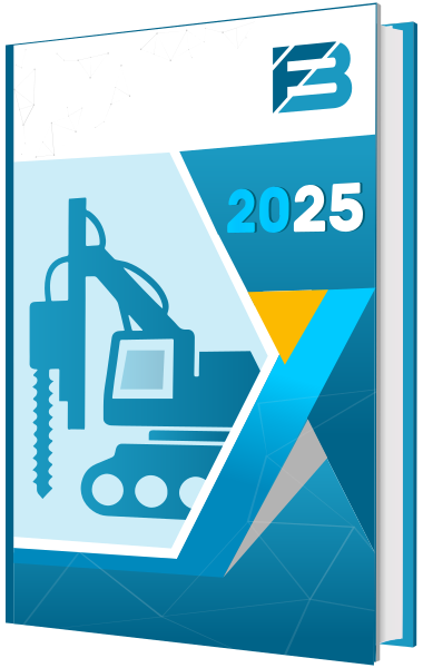
The wire bonder equipment market report provides a comprehensive evaluation of market size, revenue analysis, segment performance, regional trends, technology advancements, and competitive developments throughout the study period. The report assesses changing semiconductor assembly requirements related to bonding accuracy, process consistency, package miniaturization, interconnect reliability, material compatibility, automation, and production efficiency. The study analyzes type, bonding technology, automation and end user segment. The report further evaluates country-level demand patterns, semiconductor packaging trends, emerging bonding architectures, regulatory considerations, procurement factors, market positioning, competitive strategies, product portfolios, geographic presence, manufacturing capabilities, technological innovations, partnerships, acquisitions, and growth initiatives of leading wire bonder equipment manufacturers.
Request for Customization to gain extensive market insights.
Report Scope & Segmentation
| ATTRIBUTE | DETAILS |
| Study Period | 2021-2034 |
| Base Year | 2025 |
| Estimated Year | 2026 |
| Forecast Period | 2026-2034 |
| Historical Period | 2021-2024 |
| Growth Rate | CAGR of 7.7% from 2026-2034 |
| Unit | Value (USD Million) |
| Segmentation | By Type, Bonding Technology, Automation, End User, and Region |
| By Type |
|
| By Bonding Technology |
|
| By Automation |
|
| By End User |
|
| By Region |
|
Research Methodology
1. Bottom Up Approaches
Approach 1: Revenues and Market Share of Major Wire Bonder Equipment Players
- Collection of wire bonder equipment-specific revenues from annual reports, investor presentations, regulatory filings, earnings releases, product portfolios, technical documents, company websites, and official disclosures.
- Analysis of leading manufacturers such as Kulicke & Soffa Industries, ASMPT Limited, Besi N.V., Shinkawa Ltd., Palomar Technologies, Hesse GmbH, West-Bond Inc., F&K Delvotec Bondtechnik, DIAS Automation, TPT Wire Bonder, Hybond, FiconTEC Service, Micro Assembly Technologies, and MRSI Systems.
- Estimation of company revenues based on wire bonder portfolio breadth, Type, Bonding Technology, Automation level, End User exposure, geographic presence, installed equipment base, manufacturing footprint, and semiconductor customer relationships.
- Assessment of company offerings across ball bonders, wedge bonders, stud-bump bonders, fine-pitch bonding systems, heavy-wire bonding equipment, power semiconductor bonding solutions, and specialized semiconductor assembly platforms.
- Segregation of wire bonder equipment revenues from semiconductor devices, wafer fabrication equipment, die attach equipment, flip-chip bonding systems, hybrid bonding equipment, bonding wire materials, semiconductor packaging services, maintenance contracts, and unrelated semiconductor equipment revenues.
- Exclusion of installation services, engineering services, software-only offerings, distributor margins, refurbished equipment sales, and aftermarket consumables not included within equipment selling prices.
- Triangulation of company-level revenues with equipment shipments, average selling prices, customer application mix, regional demand patterns, and semiconductor packaging investment trends to derive global market estimates.
Approach 2: Equipment Shipment and ASP Analysis
- Estimation of global wire bonder equipment shipments across ball bonders, wedge bonders, stud-bump bonders, and specialized bonding systems.
- Collection and assessment of equipment shipment indicators including production capacity additions, semiconductor packaging investments, OSAT expansions, IDM packaging requirements, and equipment order trends.
- Development of average selling price ranges based on bonding type, automation level, throughput capability, wire compatibility, package complexity, and application requirements.
- Mapping of equipment demand across Integrated Device Manufacturers (IDMs), Outsourced Semiconductor Assembly and Testing (OSATs), automotive semiconductor manufacturers, memory producers, power semiconductor suppliers, MEMS manufacturers, LED packaging companies, and specialty semiconductor producers.
- Assessment of demand drivers including AI semiconductor production, high-bandwidth memory packaging, automotive electronics, electric vehicle semiconductors, power devices, industrial electronics, and sensor applications.
- Multiplication of estimated equipment shipments by manufacturer-level ASP assumptions to derive regional and country-level revenues.
- Aggregation of country-level estimates to calculate regional and global market values.
- Reconciliation of shipment-derived revenues with company-revenue-based estimates to minimize overestimation and underestimation.
Approach 3: Installed-Base and Replacement-Demand Model
- Estimation of the global installed base of wire bonding equipment across semiconductor fabrication companies, IDMs, OSAT facilities, research institutions, and specialty packaging manufacturers.
- Segmentation of installed equipment base by Ball Bonders, Wedge Bonders, Stud-Bump Bonders, Automation level, application category, equipment generation, and geographic region.
- Assessment of replacement cycles based on machine age, semiconductor package evolution, productivity requirements, equipment utilization rates, technology migration, and process capability limitations.
- Evaluation of replacement demand arising from outdated bonding platforms, migration toward copper wire bonding, fine-pitch requirements, automation upgrades, and yield-improvement initiatives.
- Estimation of equipment demand from new semiconductor packaging facilities, brownfield expansions, capacity upgrades, and manufacturing localization initiatives.
- Application of equipment ASP assumptions based on bonding technology, automation level, throughput, and application complexity.
- Exclusion of refurbished equipment transactions, used equipment sales, semiconductor packaging service revenues, and non-equipment aftermarket activities.
- Reconciliation of installed-base-derived demand with shipment-based and company-revenue estimates.
2. Top Down Approaches
Approach 1: Semiconductor Packaging Industry Expenditure Analysis
- Analysis of semiconductor industry growth, semiconductor assembly and packaging expenditure, OSAT capacity expansion, IDM packaging investments, and semiconductor equipment capital spending trends.
- Estimation of the proportion of semiconductor packaging equipment expenditure attributable specifically to wire bonding systems.
- Allocation of expenditure across Ball Bonders, Wedge Bonders, Stud-Bump Bonders, Thermosonic Bonding, Ultrasonic Bonding, Thermocompression Bonding, and other bonding technologies.
- Assessment of market penetration based on semiconductor package volumes, wire bonding adoption rates, package complexity, device miniaturization, and application requirements.
- Evaluation of demand contribution from memory, logic, analog, automotive semiconductors, power devices, MEMS, sensors, LEDs, and advanced semiconductor applications.
- Comparison of top-down estimates with shipment-based, installed-base, and company-revenue models to finalize the market size.
3. List of Key Sources
- Annual reports, investor presentations, earnings releases, SEC filings, and financial disclosures of wire bonder equipment manufacturers
- Company websites, product catalogues, technical datasheets, application notes, press releases, and equipment brochures
- Semiconductor Industry Association (SIA)
- SEMI
- International Semiconductor Industry Association (ISIA)
- JEDEC Solid State Technology Association
- IPC and International Electrotechnical Commission (IEC)
- International Organization for Standardization (ISO)
- World Semiconductor Trade Statistics (WSTS)
- UN Comtrade and International Trade Centre
- World Bank, OECD, UNIDO, International Energy Agency (IEA), and International Renewable Energy Agency (IRENA)
- S. Census Bureau, Bureau of Economic Analysis, Eurostat, Japan Statistics Bureau, China National Bureau of Statistics, Taiwan Ministry of Economic Affairs, and Statistics Korea
- Semiconductor equipment shipment databases and industry production statistics
- Manufacturer technical literature covering bonding technology, automation capabilities, process control, and semiconductor packaging applications
4. Primary Interviews
Supply Side Interviews: 60%
- Key Respondents:
- Wire bonder equipment manufacturers
- Semiconductor assembly and packaging equipment suppliers
- Ball bonder and wedge bonder manufacturers
- Semiconductor equipment product managers
- Sales and regional business heads
- Application engineers and process specialists
- R&D engineers involved in bonding technology development
- Manufacturing and quality-control specialists
- Semiconductor equipment distributors and channel partners
- Semiconductor packaging technology consultants
Demand Side Interviews: 40%
- Key Respondents:
- Integrated Device Manufacturers (IDMs)
- Outsourced Semiconductor Assembly and Testing (OSATs)
- Semiconductor packaging companies
- Memory semiconductor manufacturers
- Automotive semiconductor suppliers
- Power semiconductor manufacturers
- MEMS and sensor manufacturers
- LED packaging companies
- Electronics manufacturing service providers
- Semiconductor research institutes
- Procurement, sourcing, manufacturing, and process-engineering managers
Frequently Asked Questions
According to Fortune Business Insights, the global market value is expected to stand at USD 1,186.2 million in 2026 and reach USD 2,140.9 million by 2034.
In 2025, the Asia Pacific’s market value stood at USD 908.9 million.
The market is expected to exhibit a CAGR of 7.7% during the forecast period (2026-2034).
By end user, the Outsourced Semiconductor Assembly and Testing (OSATs) segment leads the market.
Rising semiconductor packaging demand, automotive electronics growth, AI computing, power devices, and automated bonding adoption drive market expansion.
Kulicke & Soffa Industries, Inc., ASMPT Limited, Besi N.V., F&K Delvotec Bondtechnik GmbH, and Hesse GmbH are among the leading players in the market.
Asia Pacific held the largest market share in 2025.
- 2021-2034
- 2025
- 2021-2024
- 140
Get 30-60 hrs Free Customization
Expand Regional and Country Coverage, Segments Analysis, Company Profiles, Competitive Benchmarking, and End-user Insights.














Related Reports
-
US +1 833 909 2966 ( Toll Free )
-
Get In Touch With Us