Semiconductor Assembly and Packaging Equipment Market Size, Share & Industry Analysis, By Type (Die Bonders, Wire Bonders, Packaging Equipment, and Others), By Application (IDMs and OSAT), By End-Use Industry (Consumer Electronics, Automotive Electronics, Industrial Electronics, Medical Devices, Aerospace and Defense, and Others), and Regional Forecast, 2026–2034
SEMICONDUCTOR ASSEMBLY AND PACKAGING EQUIPMENT MARKET SIZE AND FUTURE OUTLOOK
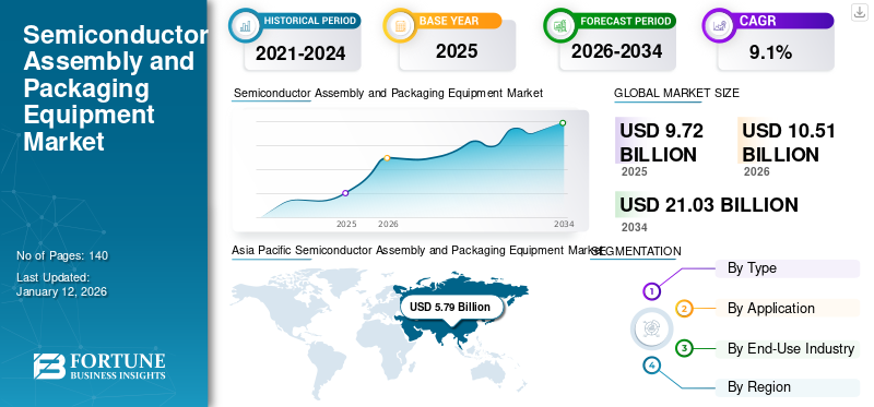
The global semiconductor assembly and packaging equipment market size was valued at USD 9.72 billion in 2025. The market is projected to grow from USD 10.51 billion in 2026 to USD 21.03 billion by 2034, exhibiting a CAGR of 9.1% during the forecast period. Asia Pacific dominated the semiconductor assembly and packaging equipment market with a share of 59.6% in 2025.
The global market is experiencing strong growth, driven by rising demand for advanced packaging technologies, miniaturization, and high-performance computing. As industries such as consumer electronics, automotive, and telecommunications increasingly adopt complex semiconductor designs, the need for efficient and precise packaging solutions continues to rise. Key players in the market are focusing on automation, AI-driven defect detection, and Industry 4.0 integration to enhance production efficiency. While the COVID-19 pandemic initially disrupted supply chains, it also accelerated the push for localization and increased investments in semiconductor manufacturing, particularly in Asia Pacific and North America.
Looking ahead, the market is expected to witness sustained growth, fueled by the expansion of AI, 5G, IoT, and electric vehicles, which require advanced semiconductor packaging solutions. The shift toward heterogeneous integration, including 2.5D and 3D packaging, will further drive innovation in bonding and encapsulation technologies. Additionally, government initiatives to strengthen domestic semiconductor production in key regions will boost equipment demand. However, supply chain challenges and high capital costs may pose hurdles. Despite this, continuous R&D investments and technological advancements will keep the market on an upward trajectory, with Asia Pacific maintaining its leadership in both market share and growth rate. ASM Pacific Technology, Kulicke & Soffa Industries, BE Semiconductor Industries, TOWA Corporation, and Shinkawa Ltd are among the top players in the global market.
Download Free sample to learn more about this report.
Download Free sample to learn more about this report.
Semiconductor Assembly and Packaging Equipment Market Trends
Rise of AI and HPC Chips Drives Demand for Advanced Packaging
The growing adoption of Artificial Intelligence (AI) and High-Performance Computing (HPC) chips is significantly accelerating the demand for semiconductor packaging technologies. As AI workloads and data processing requirements grow, traditional packaging methods struggle to provide the necessary performance, power efficiency, and interconnect density. This has led to the rapid adoption of 2.5D/3D packaging, chiplet architectures, and High-Bandwidth Memory (HBM) integration, all of which require high-precision die bonding and advanced interconnect technologies.
Leading semiconductor manufacturers and OSAT providers are heavily investing in Wafer-Level Packaging (WLP), fan-out packaging, and heterogeneous integration to meet the performance demands of AI accelerators, GPUs, and data center processors. This trend is expected to drive sustained growth in the semiconductor assembly & packaging equipment market as manufacturers seek to develop cutting-edge packaging solutions that enable faster and more efficient AI-driven computing.
MARKET DYNAMICS
Market Drivers
Surging Demand for Electric Vehicles (EVs) Accelerates Semiconductor Packaging Advancements
The rapid expansion of the Electric Vehicle (EV) market is significantly driving the demand for advanced semiconductor packaging and assembly equipment, as modern EVs rely on an increasing number of semiconductor components for efficient operation. Unlike conventional Internal Combustion Engine (ICE) vehicles, EVs require high-performance power semiconductors, battery management chips, microcontrollers, and Advanced Driver-Assistance Systems (ADAS) processors, all of which demand cutting-edge packaging solutions to ensure thermal efficiency, reliability, and miniaturization. Power electronics, particularly silicon carbide (SiC) and gallium nitride (GaN)-based power devices, are becoming crucial for improving energy efficiency and extending battery range, necessitating high-density, high-reliability packaging solutions such as chip-on-wafer, flip-chip bonding, and power module packaging.
As EV manufacturers integrate more autonomous driving features, connectivity solutions, and energy-efficient powertrains, semiconductor packaging must evolve to support higher power densities and faster data processing speeds. This shift is driving investments in system-in-package (SiP) solutions, wafer-level packaging (WLP), and 3D integration, which require specialized die bonding, wire bonding, and fan-out packaging equipment. With the EV market expected to continue its double-digit growth trajectory, demand for innovative semiconductor packaging technologies will remain a key driver for the semiconductor assembly and packaging equipment market growth.
Market Restraints
High Capital Investment Requirements Limiting Market Expansion
The semiconductor assembly & packaging equipment market faces a significant restraint due to the high capital investment required for advanced packaging technologies. As the industry shifts toward 2.5D/3D packaging, Wafer-Level Packaging (WLP), and heterogeneous integration, manufacturers must invest in cutting-edge die bonding, wire bonding, and advanced interconnect technologies, which involve high initial costs. Setting up state-of-the-art assembly and packaging facilities demands substantial spending on cleanroom infrastructure, precision automation, and high-tech testing equipment, making it challenging for smaller players and new entrants to compete with established industry leaders.
Additionally, the long development and qualification cycles for advanced semiconductor packaging solutions further strain capital resources, as companies must ensure reliability, performance, and compliance with stringent industry standards before commercial deployment. The rising cost of skilled labor, raw materials, and ongoing R&D efforts further exacerbates financial pressures, particularly in regions where government incentives for semiconductor manufacturing are limited. As a result, many smaller OSAT providers and IDMs struggle to scale operations, leading to market consolidation, where only financially robust players can sustain long-term growth and innovation in semiconductor assembly and packaging equipment technologies.
Market Opportunities
Government Incentives and Localization Efforts Drives New Investments
The increasing focus on semiconductor self-sufficiency and localization presents a significant opportunity for the semiconductor assembly & packaging equipment market. Governments worldwide are offering substantial incentives, subsidies, and funding to strengthen their domestic semiconductor ecosystems, reducing reliance on foreign supply chains. Initiatives such as the U.S. CHIPS Act, the European Chips Act, and China’s semiconductor investment programs are driving large-scale investments in semiconductor manufacturing, including assembly and packaging facilities. As a result, new IDM and OSAT facilities are being established, leading to increased demand for die bonders, wire bonders, and wafer-level packaging equipment.
Moreover, geopolitical tensions and trade restrictions are pushing companies to diversify their supply chains and set up regional packaging hubs, particularly in North America, Europe, and Southeast Asia. Countries such as India, Vietnam, and Malaysia are emerging as attractive destinations for semiconductor packaging investments due to government incentives, lower production costs, and growing technical expertise. This trend is expected to boost demand for next-generation packaging technologies as companies look to establish secure, efficient, and scalable assembly and testing facilities, creating long-term growth opportunities for semiconductor packaging equipment manufacturers.
IMPACT OF SUSTAINABILITY
Rising Sustainability Demands Driving Innovation in Semiconductor Assembly and Packaging
The increasing focus on sustainability is reshaping the global semiconductor assembly and packaging equipment industry, pushing manufacturers to adopt eco-friendly practices. Governments and industry bodies are enforcing stricter environmental regulations, such as reducing hazardous materials, minimizing waste, and improving energy efficiency. As a result, equipment manufacturers are integrating greener technologies, including low-power-consuming machinery, recyclable packaging materials, and water-saving processes, to comply with evolving standards.
This shift is also driven by consumer and corporate demand for greener electronics, compelling semiconductor firms to align with carbon neutrality goals. Companies investing in sustainable packaging solutions, such as bio-based materials and advanced thermal management techniques, are gaining a competitive edge. However, these changes require significant capital investment, which could challenge smaller players in the market. Ultimately, sustainability is not just a compliance factor but a key driver of innovation, shaping the future of semiconductor assembly and packaging.
SEGMENTATION ANALYSIS
By Type
Rising Demand for Advanced Packaging Technologies Drives Dominance of Packaging Equipment
Based on type, the market is segmented into die bonders, wire bonders, packaging equipment, and others.
Packaging equipment holds the highest share and the highest CAGR in the global market for semiconductor assembly and packaging equipment. This dominance is driven by the growing adoption of advanced packaging technologies such as fan-out wafer-level packaging (FOWLP), system-in-package (SiP), and 2.5D/3D packaging, which require sophisticated encapsulation, molding, and substrate bonding solutions. The increasing demand for high-performance computing (HPC), AI chips, and heterogeneous integration is further fueling investments in wafer-level packaging and flip-chip technology, which rely heavily on advanced packaging equipment. Additionally, electrification in automotive, 5G deployment, and edge computing are driving demand for compact, high-density semiconductor packages, reinforcing the need for precision packaging solutions.
Die bonders follow closely in terms of market share and growth due to their critical role in ensuring high-speed, high-accuracy placement of semiconductor dies onto substrates or wafers. With the rise of multi-chip packaging, chiplet architectures, and power semi-conductor devices, demand for high-precision die-bonding equipment has surged. This segment is expected to hold 30% of the market share in 2024.
Wire bonders, while still essential for traditional semiconductor packaging, are witnessing relatively slower growth due to the shift toward flip-chip bonding and wafer-level packaging. However, they continue to hold significance in cost-sensitive applications, particularly in legacy semiconductor packaging, automotive electronics, and industrial devices.
The others segment includes miscellaneous bonding, encapsulation, and inspection equipment, which play a supporting role in the assembly and packaging process. This category experiences stable demand from niche applications and specialized packaging requirements but holds a smaller share compared to the core packaging and bonding equipment segments.
To know how our report can help streamline your business, Speak to Analyst
By Application
Rising In-House Packaging Capabilities Drive IDM Dominance
Based on application, the market is segmented into IDMs and OSAT.
IDMs (Integrated Device Manufacturers) hold the highest share and the highest CAGR in the global market for semiconductor assembly and packaging equipment. This is primarily due to their increasing focus on in-house packaging and testing capabilities, reducing dependence on OSAT (Outsourced Semiconductor Assembly and Test) providers. Their dominance can also be attributed to their ability to control the entire semiconductor value chain—from chip design and fabrication to packaging and testing.
OSAT (Outsourced Semiconductor Assembly and Test) providers, while crucial for the semiconductor ecosystem, hold a comparatively lower market share. They primarily serve fabless semiconductor companies and IDMs that outsource packaging processes, making them more susceptible to market fluctuations and pricing pressures. However, OSATs remain vital for cost-effective, high-volume packaging solutions, particularly in consumer electronics and mid-range semiconductor applications. The OSAT segment is projected to acquire 40% of the market share in 2025.
By End-Use Industry
Consumer Electronics Dominates Owing to High Production Volumes of Smartphones and Laptops
By end-use industry, the market is divided into consumer electronics, automotive electronics, industrial electronics, medical devices, aerospace and defense, and others.
Consumer electronics holds the highest share of the global market for semiconductor assembly and packaging equipment. This dominance is driven by the high production volumes of smartphones, laptops, tablets, wearables, and smart home devices, all of which require advanced semiconductor packaging solutions.
Automotive electronics holds the highest CAGR, fueled by the rapid electrification of vehicles, the rise of autonomous driving, and increasing semiconductor content in modern cars. The shift toward Electric Vehicles (EVs), advanced driver-assistance systems (ADAS), and in-car connectivity is driving demand for high-reliability, thermally efficient semiconductor packaging. The segment is projected to hold 22% of the market share in 2025.
Industrial electronics holds a significant share in the market due to the increasing adoption of automation, robotics, and IoT-driven industrial applications. At the same time, medical devices are witnessing high growth, driven by wearable health monitors, imaging equipment, and implantable medical electronics. The need for miniaturized, high-performance chips in medical applications is pushing advancements in biocompatible and hermetic packaging solutions. Aerospace & defense relies on high-reliability, radiation-hardened semiconductor packaging for mission-critical applications in avionics, satellite communications, and defense electronics.
Medical devices segment is projected to exhibit a CAGR of 9.41% during the forecast period.
Semiconductor Assembly and Packaging Equipment Market Regional Outlook
By region, the market is studied across North America, Europe, Asia Pacific, South America, and the Middle East & Africa.
Asia Pacific
Asia Pacific Semiconductor Assembly and Packaging Equipment Market Size, 2025 (USD Billion)
To get more information on the regional analysis of this market, Download Free sample
The Asia Pacific region captured 59.60% of the global market in 2025, generating USD 5.79 billion in revenue, and is projected to reach USD 6.33 billion in 2026. Asia Pacific dominates, accounting for the largest semiconductor assembly and packaging equipment market share and the highest CAGR. The region’s leadership is driven by China, Taiwan, South Korea, and Japan, which serve as global hubs for semiconductor manufacturing and packaging. Government incentives, strong investments in chip fabrication, and the presence of major IDMs and OSATs fuel market growth. Additionally, the rise of AI, 5G, and Electric Vehicles (EVs) is boosting demand for advanced packaging technologies. The regional market value in 2025 was USD 5.79 billion, and in 2026, the market value led the region by USD 6.33 billion.
China is the largest player in the Asia Pacific semiconductor assembly & packaging equipment market, accounting for a significant share of global OSAT operations. The country is home to major packaging firms, such as JCET, Tongfu Microelectronics (TFME), and Hua Tian Electronics, which are expanding their advanced packaging capabilities in response to U.S. trade restrictions. The market value in China is expected to be USD 3.07 billion in 2026.
On the other hand, India is projecting to hit USD 0.61 billion in 2026. and Japan is likely to hold USD 0.48 billion in 2026.
With the U.S. imposing export controls on high-end semiconductor technologies, China has accelerated domestic semiconductor investments under its “Made in China 2025” strategy. This includes massive funding for wafer-level packaging (WLP), flip-chip bonding, and 2.5D/3D integration technologies. The Chinese government is also subsidizing local semiconductor equipment manufacturers to reduce reliance on U.S. and European suppliers.
To know how our report can help streamline your business, Speak to Analyst
North America
NNorth America contributed approximately USD 1.96 billion to the global market in 2025, accounting for 20.20% share, and is expected to reach USD 2.11 billion in 2026. exhibiting the second-fastest growing CAGR of 7.66% during the forecast period, supported by major IDM players such as Intel, Texas Instruments, and Micron. The region is experiencing a resurgence in semiconductor manufacturing due to the CHIPS Act, which aims to reduce reliance on Asian suppliers and boost local packaging and testing capabilities. Advanced semiconductor packaging, such as embedded multi-die interconnect bridge (EMIB) and 3D stacking, is gaining traction among U.S. semiconductor firms. The expansion of OSAT operations by companies, such as Amkor and ASE, in the U.S. further strengthens North America’s semiconductor assembly ecosystem. The U.S. market size is estimated to be USD 1.47 billion in 2026.
Europe
In 2025, the Europe market stood at USD 1.41 billion, representing 14.50% of global demand, and is projected to grow to USD 1.5 billion in 2026. Europe plays a vital role in the semiconductor assembly & packaging equipment market, driven by the automotive and industrial electronics sectors. Countries such as Germany, the Netherlands, and France are investing in power electronics and MEMS packaging solutions to support EVs, automation, and Industry 4.0 applications. Germany’s Infineon and Bosch are leading in power semiconductor packaging, while STMicroelectronics (France-Italy) is advancing SiC and GaN power devices. The European Chips Act is expected to strengthen the region’s semiconductor capabilities, with a focus on advanced node packaging and localization of supply chains. The market value in U.K. is expected to be USD 0.25 billion in 2026.
On the other hand, Germany is projecting to hit USD 0.57 billion in 2026. France is likely to hold USD 0.11 billion in 2025.
Middle East & Africa
In 2025, Middle East & Africa generated USD 0.31 billion, contributing 3.20% to global market revenue, and is projected to grow to USD 0.33 billion in 2026. While the Middle East & Africa holds a relatively small market share, the region is witnessing growing investments in data centers, telecommunications, and smart infrastructure. Saudi Arabia and UAE are leading digital transformation efforts, which are driving the demand for enhanced-performance computing, AI, and semiconductor chips. Governments in these countries are launching initiatives to localize semiconductor assembly and attract global players. While there is limited local semiconductor packaging activity, partnerships with global chip manufacturers are expected to foster future growth. South Africa also plays a role in semiconductor research, but large-scale packaging operations are still at a nascent stage. The GCC market size is estimated to be USD 0.80 billion in 2025.
South America
South America has a smaller market share, with demand primarily coming from consumer electronics, industrial applications, and automotive electronics. Brazil and Mexico are the key markets, with Mexico benefiting from its proximity to the U.S. semiconductor supply chain. Brazil has some local semiconductor assembly capabilities, particularly in smartcards and RFID chip packaging, but the region remains dependent on imports for advanced semiconductor technologies. Government incentives for electronics manufacturing in Mexico are helping to attract investment in semiconductor packaging, but growth remains modest compared to other regions.
Latin America recorded a market size of USD 0.25 billion in 2025, capturing 2.50% of the global market share, and is projected to reach USD 0.26 billion in 2026.
COMPETITIVE LANDSCAPE
KEY INDUSTRY PLAYERS
Technological Innovations and Strategic Expansion Drives Market Leadership
Leading players in the global semiconductor assembly and packaging equipment market are heavily investing in advanced packaging technologies, such as wafer-level packaging, fan-out packaging, 2.5D/3D IC packaging, and flip-chip bonding, to meet the growing demand for high-performance computing and miniaturization. They offer a diverse product portfolio covering die bonders, wire bonders, encapsulation systems, dicing equipment, and wafer thinning solutions, catering to industries such as consumer electronics, automotive, and telecommunications. Strong collaborations with IDMs, OSAT providers, and foundries help these companies customize solutions, optimize yield, and enhance efficiency. With a global presence across semiconductor hubs in Asia Pacific, North America, and Europe, they are well-positioned to manage supply chain complexities. Additionally, comprehensive after-sales services, including process optimization and equipment upgrades, ensure strong customer retention and long-term adoption of their technologies.
List of Key Semiconductor Assembly and Packaging Equipment Profiled:
- ASMPT (Singapore)
- Kulicke and Soffa Industries, Inc. (Singapore)
- Besi (Netherlands)
- TOWA Corporation (Japan)
- SHINKAWA Electric Co., Ltd. (Japan)
- Hana Micron (South Korea)
- SUSS MicroTec SE (Germany)
- ASM International (U.S.)
- Disco Corporation (Japan)
- Advantest Corporation (Japan)
- Tokyo Electron Limited (Japan)
- Amkor Technology (U.S.)
- Screen Holdings Co. Ltd (Japan)
- ROHM Co., Ltd. (India)
- NAURA Technology Group Co., Ltd. (China)
KEY INDUSTRY DEVELOPMENTS
- October 2024: KR made a preliminary, non-binding offer to acquire ASMPT, a prominent player in semiconductor assembly equipment. This potential acquisition reflects ongoing consolidation within the industry as companies seek to expand their market presence.
- August 2024: Indian opto-semiconductor supplier, Polymatech acquired a U.S.-based semiconductor equipment provider that specializes in packaging and testing. This acquisition is part of Polymatech's strategy to establish an integrated chipmaking business across various sectors.
- June 2023: Micron Technology announced that it is set to invest over USD 1 billion in a new chip packaging facility in India. This investment is part of a broader strategy to bolster domestic semiconductor manufacturing capabilities in the country and represents a significant move within the advanced packaging sector.
- March 2023: Samsung Electronics announced plans to invest approximately USD 230 billion in the development of an advanced semiconductor facility in South Korea. This initiative is part of a broader strategy to establish a major semiconductor hub in the country and is expected to significantly contribute to market growth throughout the forecast period. The investment will support the construction of multiple chip factories and is aligned with the South Korean government's efforts to enhance the nation's semiconductor manufacturing capabilities.
- November 2022: Lam Research Corp. acquired SEMSYSCO GmbH, enhancing its capabilities in advanced chip packaging for high-performance computing and AI applications. The financial details of the acquisition were not disclosed, but it aims to strengthen Lam Research's offerings in logic chips and chiplet-based solutions.
INVESTMENT ANALYSIS AND OPPORTUNITIES
The global semiconductor assembly and packaging equipment market presents a strong investment landscape driven by the rising demand for advanced packaging solutions, increased semiconductor production, and ongoing technological advancements. With the growing adoption of 3D packaging, fan-out wafer-level packaging (FOWLP), and system-in-package (SiP) technologies, major players and new entrants are actively investing in R&D, automation, and AI-driven packaging solutions to enhance efficiency and reduce costs. The expansion of 5G networks, AI, IoT, and high-performance computing (HPC) is further fueling the demand for sophisticated semiconductor packaging, creating substantial opportunities for equipment manufacturers.
Asia Pacific, particularly China, Taiwan, and South Korea, remains the dominant investment hub due to the presence of key semiconductor manufacturing clusters and government initiatives supporting local semiconductor production. North America and Europe are also witnessing increased investments, driven by efforts to localize semiconductor supply chains and reduce dependency on Asian markets. Additionally, the shift toward sustainable and energy-efficient packaging processes is opening new avenues for investment in eco-friendly equipment solutions. Despite supply chain disruptions and geopolitical challenges, the market remains highly lucrative for investors, especially in automation-driven packaging equipment and AI-integrated semiconductor assembly solutions, which are expected to shape the next phase of industry growth.
REPORT COVERAGE
The report provides a detailed analysis of the market and focuses on key aspects such as leading companies, product types, and leading applications of the product. Besides, it offers insights into the market trends and highlights key industry developments. In addition to the factors above, it encompasses several factors that contributed to the growth of the market in recent years.
Request for Customization to gain extensive market insights.
REPORT SCOPE & SEGMENTATION
|
ATTRIBUTE |
DETAILS |
|
Study Period |
2021-2034 |
|
Base Year |
2025 |
|
Forecast Period |
2026-2034 |
|
Historical Period |
2021-2024 |
|
Growth Rate |
CAGR of 9.1% from 2026 to 2034 |
|
Unit |
Value (USD Billion) |
|
Segmentation |
Type, Application, End-Use Industry and Region |
|
Segmentation |
By Type
By Application
By End-Use Industry
By Region
|
|
Companies Profiled in the Report |
Kulicke and Soffa Industries, Inc., Besi, TOWA Corporation, SHINKAWA Electric Co., Ltd., Hana Micron, SUSS MicroTec SE, ASMPT (Singapore), ASM International (U.S.), Disco Corporation, Advantest Corporation |
Frequently Asked Questions
The market is projected to record a valuation of USD 21.03 billion by 2034.
In 2025, the market was valued at USD 9.72 billion.
The market is projected to grow at a CAGR of 9.1% during the forecast period of 2026-2034.
The packaging equipment segment is expected to lead the market.
Surging demand for Electric Vehicles (EVs) is the key factor driving market growth.
ASM Pacific Technology, Kulicke & Soffa Industries, BE Semiconductor Industries, TOWA Corporation, Shinkawa Ltd, Hana Micron, SUSS Microtec, ASM International, Disco Corporation, Advantest Corporation and others are the top players in the market.
Asia Pacific holds the highest market share.
By application, IDMs are expected to grow with the highest CAGR during the forecast period.


- 2021-2034
- 2025
- 2021-2024
- 140
Get 30-60 hrs Free Customization
Expand Regional and Country Coverage, Segments Analysis, Company Profiles, Competitive Benchmarking, and End-user Insights.
Related Reports
-
US +1 833 909 2966 ( Toll Free )
-
Get In Touch With Us