Interposer and Silicon Bridge Market Size, Share & Industry Analysis, By Technology Type (Silicon Interposer, Silicon Bridge, and Hybrid Interposer-Bridge), By Packaging Architecture (2.5D Packaging, 3D/3.5D Packaging, and Fan-Out Embedded Bridge), By Application (AI Accelerators, Automotive, Networking and Data Center Processors, Graphics Processor Units, and Others), and Regional Forecast, 2026 – 2034
INTERPOSER AND SILICON BRIDGE MARKET SIZE AND FUTURE OUTLOOK
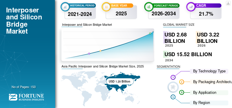
The global interposer and silicon bridge market size was valued at USD 2.68 billion in 2025 and is projected to grow from USD 3.22 billion in 2026 to USD 15.52 billion by 2034, exhibiting a CAGR of 21.7% during the forecast period. Asia Pacific dominated the interposer and silicon bridge market with a market share of 44.77% in 2025.
Silicon bridge and interposer technology includes advanced semiconductor packaging techniques that create interconnects between several chips in a single package using multiple silicon interposer or embedded silicon bridge structures by enabling chip-to-chip communication at high speed. High-speed chip-to-chip communication is particularly common for devices such as AI processors, GPUs, and high-performance computers. The market growth is driven by the rapid rise in AI and high-performance computing processors, which require advanced packaging technologies to integrate multiple chips and high-bandwidth memory into a single package for faster data transfer and improved performance.
Furthermore, many key market players, such as TSMC, Intel Corporation, Samsung Electronics, ASE Group, and Amkor Technology operating in the market, are focusing on expanding advanced packaging capabilities. They are also forming strategic partnerships with AI chip designers to scale the production of silicon interposer and bridge technologies for high-performance semiconductor applications.
Download Free sample to learn more about this report.
INTERPOSER AND SILICON BRIDGE MARKET KEY TAKEAWAYS
- 2025 Market Size: USD 2.68 Billion
- 2026 Market Size: USD 3.22 Billion
- 2034 Forecast Market Size: USD 15.52 Billion
- CAGR: 21.7% from 2026–2034
- Asia Pacific dominated the interposer and silicon bridge market with a market share of 44.77% in 2025.
- The silicon bridge segment is anticipated to grow at the highest CAGR of 25.4% over the forecast period.
- The 3D/3.5D packaging segment is anticipated to grow at the highest CAGR of 25.2% over the forecast period.
North America
North America is estimated to reach USD 0.88 billion in 2026 and secure the position of the second-largest region in the market.
Europe
The Europe market is projected to grow at a CAGR of 20.4% over the forecast period, which is the third-highest among all regions, and reach a valuation of USD 0.67 billion by 2026.
Asia Pacific
Asia Pacific accounted for the largest market share in 2024, valuing at USD 0.99 billion, and also maintained the leading share in 2025, with a value of USD 1.20 billion.
U.S.
The market is estimated to reach USD 0.68 billion in 2026, supported by strong demand for AI processors, advanced packaging technologies, and expanding domestic semiconductor manufacturing capabilities.
Japan
The market is estimated to reach USD 0.28 billion in 2026, driven by the country's leadership in semiconductor materials.
Read More
IMPACT OF GENERATIVE AI
Adoption of Generative AI to Accelerate the Demand for Silicon Interposer and Bridge Technologies in Advanced Packaging
The increasing demand for silicon interposers and silicon bridges is due to the requirements of high-performance AI processors requiring high memory bandwidth and high-speed chip-to-chip communication for training and inference of large language models. Packaging technologies such as these allow the integration of multiple logic dies with high-bandwidth memory in one package, resulting in better performance, better power efficiency, and increased speed of data transfers. The growing size and complexity of AI chips have led semiconductor companies to adopt interposer and bridge-based architectures to enable chiplet designs and heterogeneous integration. Advanced packaging capacity investment and the development of new packaging platforms are also being driven by this trend among foundries and OSATs. For instance,
- In April 2025, Intel Foundry engaged into a collaboration with Keysight Technologies on EMIB-T silicon bridge technology for next-generation AI and data-center solutions, indicating continued ecosystem build-out around bridge packaging.
INTERPOSER AND SILICON BRIDGE MARKET TRENDS
Shift toward Silicon Bridge and Hybrid Architectures to Enhance Scalability and Efficiency in Advanced Semiconductor Packaging
The semiconductor industry is increasingly shifting from full silicon interposers toward bridge and hybrid interconnect structures to improve scalability, reduce silicon usage, and support larger multi-die AI packages. The use of large interposers makes it increasingly difficult for chip manufacturers to maintain low overall costs and high yield rates, as chip sizes and high bandwidth memory (HBM) stacks continue to grow in size and complexity. Bridge architectures only use silicon in areas where high-density interconnects are needed, allowing for improved yield rates and more efficient package designs.
Manufacturers are also using hybrid solutions that combine RDL interposers with embedded silicon bridges, as these hybrid solutions allow for flexible chiplet integration and can accommodate larger package sizes for AI accelerators and high-performance computing processors. Over time, this trend toward bridge-based architectures and hybrid packaging platforms is likely to accelerate the adoption of these alternatives in the development of AI and HPC semiconductor designs. For instance,
- In May 2025, ASE Technology Holding announced FOCoS-Bridge with TSV, an advanced packaging platform designed to improve bandwidth, I/O density, and thermal dissipation for AI and HPC applications. This reflects the growing shift toward bridge-based packaging architectures.
MARKET DYNAMICS
MARKET DRIVERS
Download Free sample to learn more about this report.
Rising Shift toward Chiplet-based Semiconductor Designs to Fuel Market Growth
The market is largely influenced by the greater degree of use of chiplet-type semiconductor designs in areas where smaller dies are joined into one package to provide improved performance, scalability, and manufacturing yields. Due to the increasing use of chiplet-type architecture, semiconductor manufacturers are making less use of monolithic single die designs in favor of chiplet architecture, which requires the use of very high-density die-to-die interconnect, making silicon interposers and silicon bridges a critical element of semiconductor packaging technology. As semiconductor chip complexity continues to increase, chiplet-based architectures will continue to assist in reducing chip development costs and improving the flexibility of processor design, driving the adoption of chiplet architectures across data center processors, GPUs, and AI accelerators. These factors are likely to drive interposer and silicon bridge market growth. For instance,
- In November 2024, Amkor Technology and TSMC announced an expanded partnership to collaborate on advanced packaging and test in Arizona, aimed at providing a more integrated manufacturing and packaging flow for next-generation multi-die and chiplet-based semiconductor products in the U.S.
MARKET RESTRAINTS
High Packaging and Manufacturing Costs May Hinder Market Growth
Advanced semiconductor packaging solutions that use silicon interposers and silicon bridges involve a variety of complex fabrication processes, e.g. TSVs, high-density redistribution layers, and others, which significantly increase manufacturing costs relative to traditional semiconductor packaging. Large interposers, such as those used in AI accelerator or HPC processors, require significantly larger areas of silicon than do less expensive packaging technologies, and advanced substrates to build out the interposer, which further increase material and manufacturing costs. If companies decide to use these types of advanced packaging technologies, they will need to balance the advantages of using these technologies versus the cost and expense associated with their implementation. As many of the semiconductor applications and small designers are cost-sensitive, they may be limited in their options for using advanced packaging technologies.
MARKET OPPORTUNITIES
Emergence of 3D and 3.5D Advanced Packaging Platforms to Create New Opportunities for Market Growth
The growth of advanced 3D and 3.5D packaging platforms means strong growth for the market due to their ability to provide a far greater number of processors, memory, and connections in one package compared to conventional (2D) packaging. The need for increased density within a contained package is critically important to AI accelerators and high-performance computing processors as they require a means to integrate multiple chiplets and larger HBM designs without the restrictions of reticle size and board-level signal degradation.
In summary, advanced 3D and 3.5D packaging platforms are broadening the overall number of applications available to both silicon interposers and silicon bridges for next-generation semiconductor packaging. For instance,
- In January 2025, Broadcom announced the industry’s first 3.5D face-to-face (F2F) packaging technology for AI XPUs, stating that the platform combines 3D chip stacking with a smaller interposer footprint to improve performance, efficiency, and cost.
Segmentation Analysis
By Technology Type
High Demand for AI and HPC Processors to Drive Dominance of Silicon Interposer Technology
Based on technology type, the market is divided into silicon interposer, silicon bridge, and hybrid interposer-bridge.
The silicon interposer segment accounted for the largest market share in 2025 as they are being used in the majority of 2.5D advanced packaging platforms for artificial intelligence (AI) accelerators, graphics processing units (GPUs), and high-performance computing processors. These devices use extremely high-bandwidth links between logic chip(s) and high-bandwidth memory (HBM) stacks. The dense routing functionalities, low latency communication, and high reliability of their ability to integrate multiple dies will make this packaging architecture highly desirable among large AI and data center processors for packet processing (PP).
The silicon bridge segment is anticipated to grow at the highest CAGR of 25.4% over the forecast period. The technology enables cost-efficient chiplet integration and scalable high-density interconnects while using less silicon area than full interposers, making it increasingly attractive for next-generation AI and HPC semiconductor packages.
By Packaging Architecture
Widespread Adoption in AI and HBM Integration to Drive the Dominance of 2.5D Packaging Architecture
Based on packaging architecture, the market is categorized into 2.5D packaging, 3D/3.5D packaging, and fan-out embedded bridge.
The 2.5D packaging segment is anticipated to account for the largest interposer and silicon bridge market share as it is the most widely adopted architecture for integrating logic chips with high-bandwidth memory (HBM) in AI accelerators, GPUs, and high-performance computing systems. It has been demonstrated to be a mature technology in CoWoS and has high reliability and interconnect density. Therefore, it will be the most widely manufactured type of advanced semiconductor package in 2025.
The 3D/3.5D packaging segment is anticipated to grow at the highest CAGR of 25.2% over the forecast period. This architecture type enables vertical stacking and ultra-high-density integration of chiplets and memory, delivering superior performance, bandwidth, and power efficiency required for next-generation AI and HPC applications, driving segment growth.
By Application
To know how our report can help streamline your business, Speak to Analyst
Increasing Deployment of GPUs in Data Centers and Parallel Processing to Drive Segment Growth
Based on application, the market is classified into AI accelerators, automotive, networking and data center processors, graphics processor units, and others (consumer electronics).
The graphics processor units segment witnessed a dominating market share in 2025. This is owing to the increasing use of GPUs in accelerated/cloud-based computing and for parallel processing tasks. The advanced packaging technologies that GPUs require to accommodate high I/O density and efficient data movement between multiple dies will further increase the demand for interposer and silicon bridge solutions.
The AI accelerators segment is anticipated to grow at the highest CAGR of 24.0% during the forecast period. The rapid expansion of generative AI and machine learning workloads is driving the demand for specialized chips that require advanced packaging to deliver high bandwidth and compute performance.
Interposer and Silicon Bridge Market Regional Outlook
By geography, the market is categorized into North America, South America, Europe, the Middle East & Africa, and Asia Pacific.
Asia Pacific
Asia Pacific Interposer and Silicon Bridge Market Size, 2025 (USD Billion)
To get more information on the regional analysis of this market, Download Free sample
Asia Pacific accounted for the largest market share in 2024, valuing at USD 0.99 billion, and also maintained the leading share in 2025, with a value of USD 1.20 billion. The market in the Asia Pacific is expected to increase as it is the global hub for semiconductor manufacturing and advanced packaging, with key manufacturers such as TSMC, Samsung, ASE, and JCET operating large-scale facilities in the region. With a strong number of foundries, OSATs, and a well-established semiconductor supply chain, there is tremendous support for the high adoption of interposer and silicon bridge technology across AI, HPC, and data center applications. For instance,
- In April 2025, Amkor announced a strategic partnership with Intel focused on EMIB assembly, aimed at expanding advanced packaging capacity in Korea, Portugal, and the U.S. and increasing ecosystem availability for silicon bridge packaging.
These factors play a significant role in fueling the market growth.
China Interposer and Silicon Bridge Market
The China market is projected to be one of the largest worldwide, with 2026 revenues estimated at around USD 0.31 billion, representing roughly 9.6% of global sales.
To know how our report can help streamline your business, Speak to Analyst
Japan Interposer and Silicon Bridge Market
The Japan market is estimated at around USD 0.28 billion in 2026, accounting for roughly 8.7% of global revenues. This is owing to the country’s strong presence in semiconductor materials, equipment manufacturing, and advanced packaging ecosystem, which supports the product adoption in high-performance computing and AI applications.
India Interposer and Silicon Bridge Market
The India market is estimated at around USD 0.20 billion in 2026, accounting for roughly 6.2% of global revenues.
North America
North America is estimated to reach USD 0.88 billion in 2026 and secure the position of the second-largest region in the market. This is owing to the presence of established semiconductor firms and AI chip developers such as Intel, NVIDIA, and AMD, who make considerable investments in progressive packaging technologies that provide high-performance computing and artificial intelligence workload solutions. Furthermore, there has been a considerable increase in the expansion of data centers and an increase in investments made in domestic semiconductor manufacturing and packaging. This increases the product usage in the region. For instance,
- In November 2024, Amkor and TSMC announced an expanded partnership to collaborate on advanced packaging and test in Arizona, intended to provide a more integrated U.S. manufacturing and packaging flow for next-generation semiconductors.
U.S. Interposer and Silicon Bridge Market
Based on North America’s significant contribution and the U.S. dominance within the region, the U.S. market can be analytically approximated at around USD 0.68 billion in 2026, accounting for roughly 21.1% of global sales.
Europe
The Europe market is projected to grow at a CAGR of 20.4% over the forecast period, which is the third-highest among all regions, and reach a valuation of USD 0.67 billion by 2026. The European market for semiconductor packaging is observing significant growth, due to investment in European semiconductor fabrication and packaging capabilities. These investments are being made through programs such as the European Chips Act. Additionally, there is a significant presence of automotive, industrial, and high-performance computing industries that are creating the demand for new packaging technologies such as interposers and silicon bridges in Europe.
U.K Interposer and Silicon Bridge Market
The U.K. market is estimated to touch around USD 0.12 billion in 2026, representing roughly 3.7% of global revenues.
Germany Interposer and Silicon Bridge Market
The Germany market is projected to reach approximately USD 0.13 billion in 2026, equivalent to around 4.0% of global sales.
South America
South America is expected to witness moderate growth in this market during the forecast period. The South America market is set to reach a valuation of USD 0.07 billion in 2026. The regional market growth is driven by the gradual expansion of data center infrastructure and increasing adoption of cloud and AI-based services across key countries such as Brazil and Argentina. In addition, rising digital transformation initiatives and investments in telecommunications and enterprise in Brazil are supporting the demand for high-performance computing systems, indirectly contributing to the adoption of advanced packaging technologies.
Middle East and Africa
The Middle East and Africa market is estimated to reach USD 0.13 billion in 2026 and expected to grow at a prominent growth rate in the coming years. The market growth in the Middle East and Africa is driven by increasing investments in digital infrastructure, data centers, and AI initiatives across countries such as the UAE and Saudi Arabia. Additionally, the increased adoption of advanced technology had a positive impact on creating the demand for high-performance computing systems, indirectly supporting the demand for advanced packaging solutions such as interposers and silicon bridges. In the Middle East & Africa, the GCC is set to reach a value of USD 0.04 billion in 2026.
COMPETITIVE LANDSCAPE
Key Industry Players
Focus on Expanding Advanced Packaging Capabilities by Key Players to Propel Market Growth
The global interposer and silicon bridge market holds a semi-consolidated structure, with prominent players such as TSMC, Intel Corporation, Samsung Electronics, ASE Group, and Amkor Technology holding significant positions. These companies are driving market growth through continuous investments in advanced packaging technologies, including silicon interposers, embedded silicon bridge solutions, and hybrid 2.5D/3D integration platforms. Strategic initiatives such as expanding CoWoS capacity, advancing EMIB technology, and developing next-generation packaging architectures are enabling higher performance, improved bandwidth, and better power efficiency for AI and high-performance computing applications.
Other notable players in the global market include JCET Group, Siliconware Precision Industries (SPIL), Powertech Technology Inc. (PTI), Chipbond Technology, and Nepes. These companies are increasingly focusing on enhancing heterogeneous integration capabilities, improving manufacturing processes, and scaling production capacity to meet the rising demand. Strategic investments in advanced packaging facilities, innovation in chiplet-based architectures, and expansion of global manufacturing footprints are expected to strengthen their market positioning and drive growth throughout the forecast period.
LIST OF KEY INTERPOSER AND SILICON BRIDGE COMPANIES PROFILED
- Taiwan Semiconductor Manufacturing Company (TSMC) (Taiwan)
- Intel Corporation (U.S.)
- Samsung Electronics (South Korea)
- ASE Group (Taiwan)
- Amkor Technology (U.S.)
- JCET Group (China)
- GlobalFoundries (U.S.)
- Powertech Technology Inc. (PTI) (Taiwan)
- Chipbond Technology (Taiwan)
- Nepes(South Korea)
KEY INDUSTRY DEVELOPMENTS
- March 2026: Chipbond opened a new advanced semiconductor packaging and testing facility in Penang, with a reported investment of about USD 200 million as part of its global expansion strategy.
- May 2025: ASE launched FOCoS-Bridge with TSV, enhancing bandwidth, I/O density, and thermal performance for AI and HPC applications, reinforcing bridge-based packaging adoption.
- November 2024: ASE Group shared plans to increase investment in advanced packaging and testing facilities to support the rising demand for AI-driven semiconductor packaging, including bridge and heterogeneous integration solutions.
- October 2024: Samsung announced plans to expand its advanced packaging production capacity in South Korea, focusing on next-generation heterogeneous integration technologies, including interposer and bridge-based platforms.
- June 2024: TSMC announced advancements in its CoWoS roadmap, including next-generation packaging solutions to support larger AI processors and higher HBM integration, reinforcing its leadership in interposer-based technologies.
- June 2024: Nepes launched a 600mm FOPLP solution and a chipset packaging design based on a fan-out RDL interposer at ECTC 2024. Nepes is actively developing interposer-adjacent advanced packaging aimed at heterogeneous integration and AI-oriented packaging use cases.
- March 2024: JCET announced that its subsidiary JCET Automotive Electronics (Shanghai) secured a USD 600 million capital increase to support the construction of its first intelligent automotive-grade chip advanced packaging flagship factory. Through this investment, the company aims to expand its footprint in China.
REPORT COVERAGE
The global interposer and silicon bridge market analysis includes a comprehensive study of the market size & forecast by all the market segments included in the report. It includes details on the market dynamics and market trends expected to drive the market over the forecast period. It provides information on key aspects, including an overview of technological advancements, pipeline candidates, the regulatory environment, and product launches. Additionally, it details partnerships, mergers & acquisitions, as well as key industry developments and prevalence by key regions. The global market research report also provides a detailed competitive landscape with information on the market share and profiles of key operating players.
Request for Customization to gain extensive market insights.
Report Scope & Segmentation
| ATTRIBUTE | DETAILS |
| Study Period | 2021-2034 |
| Base Year | 2025 |
| Estimated Year | 2026 |
| Forecast Period | 2026-2034 |
| Historical Period | 2021-2024 |
| Growth Rate | CAGR of 21.7% from 2026-2034 |
| Unit | Value (USD Billion) |
| Segmentation | By Technology Type, Packaging Architecture, Application, and Region |
| By Technology Type |
|
| By Packaging Architecture |
|
| By Application |
|
| By Region |
|
Frequently Asked Questions
According to Fortune Business Insights, the global market value stood at USD 2.68 billion in 2025 and is projected to reach USD 15.52 billion by 2034.
In 2025, the Asia Pacific market value stood at USD 1.20 billion.
The market is anticipated to grow at a CAGR of 21.7% during the forecast period of 2026-2034.
By technology type, the silicon interposer segment led the market in 2025.
The rising shift toward chiplet-based semiconductor designs is a key factor fueling market growth.
TSMC, Intel Corporation, Samsung Electronics, ASE Group, and Amkor Technology are the major players in the global market.
Asia Pacific dominated the market in 2025.


- 2021-2034
- 2025
- 2021-2024
- 150
Get 30-60 hrs Free Customization
Expand Regional and Country Coverage, Segments Analysis, Company Profiles, Competitive Benchmarking, and End-user Insights.
Related Reports
-
US +1 833 909 2966 ( Toll Free )
-
Get In Touch With Us