Photoresist Chemicals Market Size, Share & Industry Analysis, By Type (DUV (ArF / KrF) Photoresists, g-line / i-line Photoresists, EUV Photoresists, and Others), By Application (Semiconductors, Flat Panel Displays (LCD / OLED), Printed Circuit Boards, and MEMS, Sensors & Others), By End-use Industry (Consumer Electronics, Data Centers & Computing, Automotive Electronics, Industrial & Medical, and Others), and Regional Forecast, 2026-2034
Photoresist Chemicals Market Size and Future Outlook
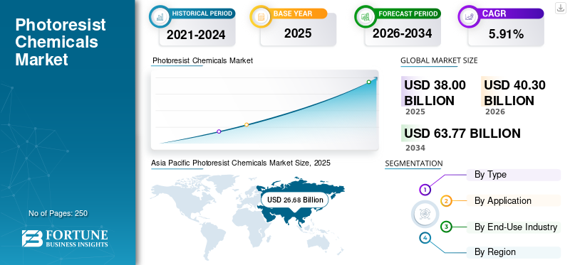
The global photoresist chemicals market size was valued at USD 38.00 billion in 2025. The market is projected to grow from USD 40.30 billion in 2026 to USD 63.77 billion by 2034, exhibiting a CAGR of 5.91% during the forecast period. Asia Pacific dominated the global photoresist chemicals market with a market share of 70.21% in 2025.
Photoresist chemicals are light-sensitive polymeric materials used in photolithography processes to transfer circuit patterns onto substrates such as silicon wafers, glass panels, and printed circuit boards. When exposed to specific wavelengths of light (UV, DUV, or EUV), photoresists undergo controlled chemical changes that allow selective removal of either exposed or unexposed areas during development, enabling precise pattern formation.
These chemicals are a critical enabler of semiconductor, display, and microelectronic manufacturing, as they determine feature resolution, pattern fidelity, and device performance. The continued expansion and increasing complexity of semiconductor manufacturing, driven by demand for advanced logic, memory, automotive, and AI-related chips are the primary factors of market growth.
- For instance, in 2025, JSR Corporation announced a strategic partnership with a major semiconductor manufacturer to co-develop next-generation photoresist materials targeting advanced fabrication processes. While this is a collaboration for future products, it signals forthcoming product innovations and qualifications.
There are several key industry players, such as Tokyo Ohka Kogyo Co., Ltd, JSR Corporation, Shin-Etsu Chemical Co., Ltd, and FUJIFILM, operating in the market, are focusing on developing various innovative products to support the rising demand.
Download Free sample to learn more about this report.
PHOTORESIST CHEMICALS MARKET TRENDS
Accelerated Adoption of Extreme Ultraviolet (EUV) Lithography is a Prominent Market Trend
The market is undergoing a structural transformation driven by rapid advancements in semiconductor manufacturing and rising lithography complexity. The most prominent trend is the accelerated adoption of extreme ultraviolet (EUV) lithography, which is increasing demand for high-performance, chemically amplified photoresists capable of achieving finer resolutions with less number of defects.
A key indicator of this trend is the accelerated adoption of extreme ultraviolet (EUV) lithography at advanced nodes (7 nm and below). EUV lithography uses a much shorter wavelength (13.5 nm) than deep ultraviolet (DUV), enabling finer feature sizes but also introducing significant technical challenges, such as stochastic defects, line-edge roughness, and sensitivity limitations. To address these issues, semiconductor manufacturers require chemically amplified EUV photoresists with highly controlled molecular structures and ultra-high purity.
Download Free sample to learn more about this report.
MARKET DYNAMICS
MARKET DRIVERS
Continued Expansion and Increasing Complexity of Semiconductor Manufacturing, Accelerates Market Growth
The continued expansion and increasing complexity of semiconductor manufacturing, particularly at advanced and mid technology nodes is a crucial factor for the photoresist chemicals market growth.
As semiconductor devices scale to smaller geometries, the number of lithography steps per wafer increases, directly raising the consumption of photoresist chemicals. Advanced nodes (≤7 nm) require extreme ultraviolet (EUV) lithography, which uses highly specialized photoresists with stringent requirements for resolution, defect control, and sensitivity. These EUV photoresists are high-value materials, significantly increasing market value even when volume growth is modest.
At the same time, strong demand for automotive, industrial, and power semiconductors is driving sustained investment in mature and mid-node fabrication, where DUV (ArF/KrF) photoresists remain essential. This dual demand structure advanced-node EUV growth and mature-node DUV expansion creates a stable and long-term growth trajectory for the market.
Therefore, growth in wafer fabrication capacity, combined with rising lithography intensity per chip, directly translates into higher demand and value growth for such chemicals.
MARKET RESTRAINTS
Lengthy, Complex, and Capital-Intensive Qualification Cycles May Restrict Market Growth
One of the most significant restraints in the market is the lengthy, complex, and capital-intensive qualification process required by semiconductor manufacturers, which slows product commercialization and limits supplier participation. Photoresists are mission-critical materials in photolithography, where microscopic inconsistencies can result in pattern defects, yield loss, or device failure. Consequently, semiconductor fabs impose extremely stringent qualification requirements before approving any new photoresist formulation for high-volume manufacturing.
The qualification process typically involves multi-stage testing, including lab-scale evaluation, pilot-line trials, defectivity analysis, yield impact assessment, and long-term process stability validation. For advanced lithography nodes particularly DUV immersion and EUV processes this evaluation can take 12 to 36 months, as photoresist performance must be verified across multiple process windows, exposure tools, and device architectures. Any formulation change, even minor adjustments to improve sensitivity or line-edge roughness, may trigger partial or full requalification.
This extended timeline significantly increases research and development costs for photoresist suppliers, as materials must be tailored to individual customer processes and exposure tools. Moreover, suppliers are often required to engage in co-development partnerships with chipmakers, allocating technical staff and resources over prolonged periods without guaranteed commercial adoption. These factors raise financial risk, particularly for smaller or new entrants.
MARKET OPPORTUNITIES
Advanced Semiconductor Packaging and Heterogeneous Integration Offers Growth Prospects
Advanced semiconductor packaging and heterogeneous integration represent a major growth opportunity, as device scaling increasingly shifts from the front-end (transistor miniaturization) to the back-end (packaging-level integration). With traditional Moore’s Law scaling becoming more complex and costly, chipmakers are adopting chiplet architectures, fan-out wafer-level packaging (FOWLP), redistribution layers (RDL), and 2.5D/3D integration to enhance performance, power efficiency, and functionality.
These packaging technologies rely heavily on high-precision lithography processes, thereby increasing demand for specialized photoresist formulations. Unlike conventional front-end resists, packaging applications require thick-film, high-aspect-ratio, and mechanically robust photoresists capable of forming fine interconnects while maintaining dimensional stability during plating, etching, and thermal cycling. As line widths in RDL processes continue to shrink, photoresists must deliver higher resolution at greater thickness, creating new technical challenges and value-added opportunities for material suppliers.
Moreover, the rapid growth of AI accelerators, high-performance computing, and data-center processors is accelerating adoption of heterogeneous integration, as these applications demand high bandwidth, low latency, and power-efficient interconnects. This directly translates into increased lithography steps and higher photoresist consumption at the packaging stage.
MARKET CHALLENGES
Supply-Chain Sensitivity to Pose a Critical Challenge to Market Growth
The photoresist supply chain is highly concentrated and vulnerable to disruption. Production relies on ultra-high-purity raw materials, specialized manufacturing equipment, and tightly controlled logistics. Any disruption, whether from raw material shortages, geopolitical tensions, or export controls can impact availability and lead times. For semiconductor manufacturers, disruptions in photoresist supply pose a significant operational risk, reinforcing conservative procurement strategies and limiting opportunities for new suppliers.
Segmentation Analysis
By Type
Increasing Wafers Adoption in LED Applications Propel Growth of DUV (ArF / KrF) Photoresists
Based on type, the market is divided into DUV (ArF / KrF) photoresists, g-line / i-line photoresists, EUV photoresists, and others.
The DUV (ArF / KrF) photoresists segment is anticipated to account for the largest photoresist chemicals market share due to their widespread adoption across mature and mid-node semiconductor manufacturing, where the majority of global wafer fabrication capacity is concentrated. Despite the growing deployment of EUV lithography at leading-edge nodes, most semiconductor production including automotive, industrial, power, and analog devices continue to rely on DUV-based processes because of their cost efficiency, process stability, and established tool infrastructure.
The g-line / i-line photoresists is the second largest segment and serves legacy semiconductor nodes and non-IC applications, where ultra-fine resolution is not a primary requirement. These photoresists are widely used in printed circuit boards (PCBs), discrete semiconductors, power devices, and specialty electronics, as well as in certain mature fabs operating at larger feature sizes.
The EUV photoresists segment is anticipated to rise with a CAGR of 6.45% over the forecast period.
By Application
Semiconductor is the Leading Application Owing to Expansion in Semiconductor Manufacturing
Based on application, the market is segmented into semiconductors, flat panel displays (LCD / OLED), printed circuit boards, and MEMS, sensors & others.
The semiconductors segment accounts for the largest market share, supported by sustained expansion of global semiconductor manufacturing.
The growing demand for advanced logic, memory, automotive, and power semiconductors has significantly increased wafer fabrication activity worldwide. Semiconductor manufacturing requires multiple lithography steps per wafer, each involving the application and removal of photoresist materials.
The printed circuit boards (PCBs) segment contributes stable demand, supported by electronics manufacturing in automotive, industrial, and consumer applications.
The flat panel displays (LCD / OLED) segment is projected to grow at a CAGR of 4.75% over the forecast period.
By End-Use Industry
To know how our report can help streamline your business, Speak to Analyst
Consumer Electronics Segment to Lead Market Due to Broad Application Base
Based on end-use industry, the market is segmented into consumer electronics, data centers & computing, automotive electronics, industrial & medical, and others.
The consumer electronics segment is anticipated to witness the largest share over the forecast period due to its large-scale production volumes and broad application base. Consumer electronics such as smartphones, tablets, laptops, televisions, and wearable devices incorporate a wide range of semiconductors, including logic chips, memory, display drivers, and power management ICs.
The data centers & computing segment represents one of the fastest-growing end-use segments, driven by the rapid expansion of cloud computing, artificial intelligence (AI), high-performance computing (HPC), and data storage infrastructure.
The data centers & computing segment is projected to grow at a highest CAGR of 6.62% over the forecast period.
Photoresist Chemicals Market Regional OutlooK
By region, the market is categorized into Europe, North America, Asia Pacific, Latin America, and the Middle East & Africa.
Asia Pacific
Asia Pacific Photoresist Chemicals Market Size, 2025 (USD Billion)
To get more information on the regional analysis of this market, Download Free sample
Asia Pacific is estimated to reach USD 28.40 billion in 2026 and will dominate the global photoresist chemicals market, accounting for the largest manufacturing and consumption of photoresist chemicals. The region hosts the majority of the world’s semiconductor foundries, memory fabs, and display manufacturing facilities, concentrated in Taiwan, South Korea, China, and Japan. Strong demand for advanced logic, memory, automotive, and consumer electronics semiconductors, combined with rapid adoption of EUV and advanced DUV lithography, drives high consumption of photoresist chemicals.
Japan Photoresist Chemicals Market
The Japan market is estimated to capture USD 4.35 billion in 2026, accounting for roughly 10.8% of global revenues. Japan plays a pivotal and strategic role in the global market, serving as both a major consumption center and the world’s leading supply base for advanced photoresist materials. The country hosts several of the most technologically advanced photoresist manufacturers, accounting for a dominant share of global supply, particularly for DUV and EUV photoresists.
China Photoresist Chemicals Market
China’s market is projected to be one of the largest worldwide, with 2026 revenues estimated at around USD 14.59 billion, representing roughly 36.2% of global sales. China represents one of the most strategically important markets, driven by its large-scale semiconductor manufacturing base, extensive electronics production, and ongoing efforts to localize critical materials. While China remains dependent on imports for leading-edge photoresists due to its dominance in mature and mid-node semiconductor fabrication, PCB manufacturing, and display production.
To know how our report can help streamline your business, Speak to Analyst
India Photoresist Chemicals Market
In 2026, the Indian market will reach USD 2.10 billion, accounting for roughly 5.2% of global revenues. India represents an emerging but small market within the global landscape, with demand largely driven by electronics manufacturing, printed circuit boards (PCBs), and research-oriented semiconductor activities rather than large-scale wafer fabrication. Currently, India lacks commercial advanced or mature semiconductor fabs, which structurally limits domestic consumption of high-end photoresists used in front-end wafer manufacturing.
North America
North America’s market size in 2024 was USD 4.71 billion and represents a significant and technologically advanced market, driven mainly by the semiconductor ecosystem in the U.S. The region is characterized by strong demand for advanced logic, high-performance computing, and data-center-related semiconductors, which rely on high-value photoresists. Recent government initiatives to strengthen domestic semiconductor manufacturing are encouraging new fab investments, which are expected to support medium- to long-term market growth.
U.S. Photoresist Chemicals Market
Based on North America’s strong contribution and the U.S. dominance within the region, the U.S. market can be analytically approximated at around USD 4.46 billion in 2026, accounting for roughly 11.1% of global sales.
Europe
Europe is projected to record a growth rate of 5.06% in the coming years and reach USD 4.08 billion by 2026. Europe’s market is driven by automotive, industrial, and power semiconductor manufacturing, with key fabrication activities located in Germany, France, Italy, and U.K. The region focuses primarily on mature and specialty semiconductor nodes, supporting steady demand for DUV and legacy photoresists. While Europe has limited presence in leading-edge logic manufacturing, growing emphasis on automotive electrification and industrial automation sustains moderate market growth.
U.K. Photoresist Chemicals Market
The U.K. market size is estimated at around USD 0.37 billion for 2026, representing roughly 0.9% of global revenues.
Germany Photoresist Chemicals Market
Germany’s market in 2026 is projected to reach approximately USD 0.97 billion, equivalent to around 2.4% of global sales.
Latin America and the Middle East & Africa
Latin America and the Middle East & Africa are expected to witness moderate growth during the forecast period. Latin America is set to reach a valuation of USD 1.26 billion in 2026. The region accounts for a relatively small share of the global market and is largely centered on assembly, testing, and PCB manufacturing, rather than wafer fabrication. As a result, demand is mainly driven by lower-end photoresists used in PCB and niche electronics applications, leading to modest growth prospects.
The Middle East & Africa is set to reach USD 1.52 billion in 2025.
GCC Photoresist Chemicals Market
The GCC market is projected to reach around USD 1.01 billion in 2026, representing roughly 2.5% of global revenues.
COMPETITIVE LANDSCAPE
Key Industry Players
Leading Companies Focus on Innovations to Capture Strong Market Share
The market is highly consolidated, especially in advanced (ArF immersion) and EUV photoresists, characterized by the presence of a limited number of large, technologically advanced manufacturers such as TOKYO OHKA KOGYO (TOK), JSR, Shin-Etsu, FUJIFILM, DuPont and a fragmented base of regional and niche suppliers. Competition is shaped primarily by technological capability, customer qualification depth, and long-term relationships with semiconductor manufacturers, rather than by pricing alone. In the market, suppliers compete on their ability to deliver high-performance, ultra-high-purity materials that meet increasingly stringent lithography requirements across DUV and EUV processes.
Other notable players in the global market include Mitsui Chemicals, Allresist GmbH, and Sumitomo Chemicals. These companies are expected to prioritize new product launches to increase their global market share during the forecast period.
LIST OF KEY PHOTORESIST CHEMICALS COMPANIES PROFILED
- Tokyo Ohka Kogyo Co., Ltd. (Japan)
- JSR Corporation (Japan)
- Shin-Etsu Chemical Co., Ltd. (Japan)
- FUJIFILM Corporation (Japan)
- DuPont de Nemours, Inc. (U.S.)
- Mitsui Chemicals, Inc. (Japan)
- Nagase & Co., Ltd. (Japan)
- Allresist GmbH (Germany)
- Sun Chemical Corporation (U.S.)
- Hubei Dinglong Co., Ltd. (China)
- Sumitomo Chemical Co., Ltd. (Japan)
KEY INDUSTRY DEVELOPMENTS
- November 2025: FUJIFILM Corporation announced the completion of a new development and evaluation facility at its Shizuoka Factory, operated by FUJIFILM Electronic Materials Co., Ltd. (FFEM), the core company driving Fujifilm’s semiconductor materials This investment enhances Fujifilm’s capabilities in performance and quality evaluation, enabling faster development of advanced and next-generation semiconductor materials while supporting a stable supply of high-quality products.
- July 2025: FUJIFILM Corporation announced the development of a PFAS-free negative-type ArF immersion photoresist for advanced semiconductor manufacturing. Developed and evaluated in collaboration with imec, the resist demonstrated high-yield performance at the 28 nm node for metal wiring used in automotive and industrial semiconductors. Fujifilm plans to advance customer evaluations and pursue early commercialization.
- February 2025: Sumitomo Chemical plans to expand its photoresist evaluation facilities at the Osaka Works to enhance development and mass-production evaluation capabilities for front-end and back-end semiconductor manufacturing processes, strengthening support for advanced semiconductor production.
- May 2024: JSR Corporation entered into a share purchase agreement to acquire Yamanaka Hutech Corporation as a wholly owned subsidiary. This acquisition expanded JSR’s semiconductor materials portfolio beyond photoresists by incorporating high-purity CVD/ALD precursor technologies, thereby enhancing its ability to deliver greater value to customers as a global semiconductor materials supplier.
- April 2024: Shin-Etsu Chemical Co., Ltd. announced that in order to expand its semiconductor lithography materials business, the company decided to build a new plant in Isesaki City in Gunma Prefecture, Japan. The new plant will become Shin-Etsu’s fourth production base for this business.
- December 2023: DIC Corporation has acquired 100% of the shares of Quebec-based PCAS Canada Inc. from French based company PCAS S.A., which manufactures and sells polymers used in photoresists for semiconductor photolithography.
- September 2021: JSR announced that it has entered into an agreement to acquire Inpria Corporation, a Corvallis, Oregon–based leader in metal oxide photoresist technologies for extreme ultraviolet (EUV) lithography. The acquisition strengthens JSR’s position in advanced semiconductor materials, as EUV lithography adoption continues to expand with ongoing scaling to smaller chip dimensions.
REPORT COVERAGE
Request for Customization to gain extensive market insights.
Report Scope & Segmentation
|
ATTRIBUTE |
DETAILS |
|
Study Period |
2021-2034 |
|
Base Year |
2025 |
|
Estimated Year |
2026 |
|
Forecast Period |
2026-2034 |
|
Historical Period |
2021-2024 |
|
Growth Rate |
CAGR of 5.91% from 2026-2034 |
|
Unit |
Value (USD Billion) |
|
Segmentation |
By Type, Application, End-Use Industry, and Region |
|
By Type |
· DUV (ArF / KrF) Photoresists · g-line / i-line Photoresists · EUV Photoresists · Others |
|
By Application |
· Semiconductors · Flat Panel Displays (LCD / OLED) · Printed Circuit Boards · MEMS, Sensors & Others |
|
By End-Use Industry |
· Consumer Electronics · Data Centers & Computing · Automotive Electronics · Industrial & Medical · Others |
|
By Region |
· North America (By Type, Application, End-Use Industry, and Country) o U.S. (By End-Use Industry) o Canada (By End-Use Industry) · Europe (By Type, Application, End-Use Industry, and Country) o Germany (By End-Use Industry) o U.K. (By End-Use Industry) o France (By End-Use Industry) o Italy (By End-Use Industry) o Rest of Europe (By End-Use Industry) · Asia Pacific (By Type, Application, End-Use Industry, and Country) o China (By End-Use Industry) o Japan (By End-Use Industry) o India (By End-Use Industry) o South Korea (By End-Use Industry) o Rest of Asia Pacific · Latin America (By Type, Application, End-Use Industry, and Country) o Brazil (By End-Use Industry) o Mexico (By End-Use Industry) o Rest of Latin America (By End-Use Industry) · Middle East & Africa (By Type, Application, End-Use Industry, and Country) o GCC (By End-Use Industry) o South Africa (By End-Use Industry) o Rest of the Middle East & Africa (By End-Use Industry) |
Frequently Asked Questions
According to Fortune Business Insights, the global market value stood at USD 38.00 billion in 2025 and is projected to reach USD 63.77 billion by 2034.
In 2025, Asia Pacifics market value stood at USD 26.68 billion.
The market is expected to exhibit a CAGR of 5.91% during the forecast period.
By type, the DUV (ArF / KrF) photoresists segment is expected to lead the market.
The increasing demand from semiconductor industry is driving market expansion.
TOKYO OHKA KOGYO (TOK), JSR, Shin-Etsu, FUJIFILM, DuPont are the major players in the global market.
Asia Pacific dominated the market in 2025 by holding the largest share.


- 2021-2034
- 2025
- 2021-2024
- 250
Get 30-60 hrs Free Customization
Expand Regional and Country Coverage, Segments Analysis, Company Profiles, Competitive Benchmarking, and End-user Insights.
Related Reports
-
US +1 833 909 2966 ( Toll Free )
-
Get In Touch With Us