AI Chip Fabrication Chemicals Market Size, Share & Industry Analysis, By Chemical Type (Patterning Chemicals, Etch & Clean Chemicals, and Deposition & Interconnect Chemicals), By Grade (Standard Grade, Advanced Node Grade, and Leading Edge Grade) By Application (AI Compute Logic, AI Memory, and AI Packaging & Interconnect), and Regional Forecast, 2026-2034
AI Chip Fabrication Chemicals Market Size and Future Outlook
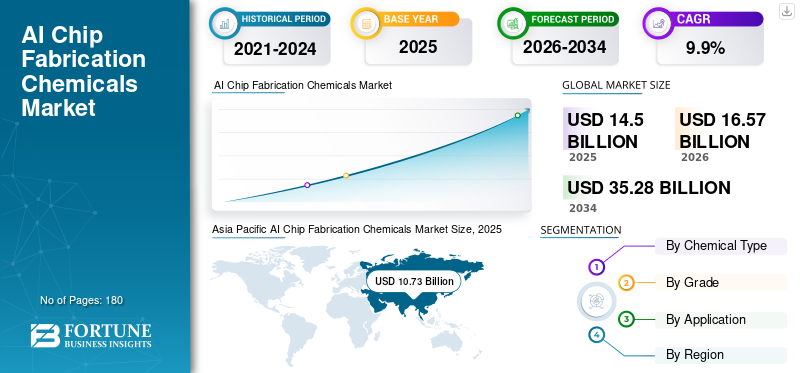
The global AI chip fabrication chemicals market size was valued at USD 14.50 billion in 2025. The market is projected to grow from USD 16.57 billion in 2026 to USD 35.28 billion by 2034, exhibiting a CAGR of 9.9% during the forecast period. Asia Pacific dominated the AI chip fabrication chemicals market with a market share of 74% in 2025.
AI chip fabrication chemicals are highly specialized process materials designed to enable ultra-precise patterning, deposition, cleaning, doping, and planarization steps in advanced semiconductor manufacturing. These chemicals include high-purity photoresists, developers, CMP slurries, wet etchants, cleaning solutions, specialty gases, and advanced deposition precursors. They play a critical role in achieving sub-5nm feature definition, multilayer interconnect formation, and defect-free wafer processing required for AI accelerators, GPUs, High-Bandwidth Memory (HBM), and advanced logic devices.
As AI chip architectures integrate more transistors, 3D stacking, chiplets, and advanced packaging technologies, the tolerance for contamination, line edge roughness, and material variability continues to shrink. Therefore, there is a sustained high demand for ultra-high-purity, tightly controlled fabrication raw materials that ensure yield stability, performance optimization, and long-term device reliability. Generative AI (GenAI) is driving the market for AI chip fabrication chemicals as the demand for advanced semiconductors accelerates, which in turn necessitates higher volumes, increased purity, and novel formulations of specialized chemicals for fabrication.
The global market is shaped by a concentrated group of specialty chemical and materials suppliers with deep expertise in semiconductor-grade purification, molecular design, and process integration, supported by leading-edge lithography and etch systems. Key players include JSR Corporation, FUJIFILM Electronic Materials, Fujimi Corporation, Merck, and AGC Inc. Their product portfolios span EUV-compatible photoresists, advanced wet cleans, ALD/CVD precursors, high-selectivity etchants, and defect-optimized CMP materials tailored for advanced logic, AI memory, and advanced packaging applications. Continuous collaboration with leading foundries and integrated device manufacturers, alongside investments in contamination control, sustainable formulations, and next-generation EUV materials, continues to strengthen their competitive positioning in the AI-driven semiconductor ecosystem.
Download Free sample to learn more about this report.
AI CHIP FABRICATION CHEMICALS MARKET TRENDS
Expansion of AI-Focused Fabs and Advanced Packaging Facilities Accelerates Specialty Chemical Consumption
The continued expansion of AI-focused semiconductor fabrication plants and advanced packaging facilities is a key trend driving global demand for AI chip fabrication chemicals. Foundries and integrated device manufacturers are scaling up capacity for advanced logic nodes, High-Bandwidth Memory (HBM), and chiplet-based architectures to support chemical processes, high performance computing, and data center acceleration. These facilities operate at high wafer throughput and incorporate complex multi-patterning, EUV lithography, advanced etch, deposition, and cleaning processes that require a broad portfolio of ultra-high-purity chemicals.
- For instance, in April 2025, TSMC announced continued capacity expansion for advanced 3nm and 2nm nodes to support AI and HPC applications, reinforcing demand for next-generation EUV materials and high-purity process chemicals.
MARKET DYNAMICS
MARKET DRIVERS
Download Free sample to learn more about this report.
Advanced Node Scaling and AI-Driven Chip Complexity to Drive Market Growth
Ongoing semiconductor scaling and the rising architectural complexity of AI chips remain fundamental drivers of demand for fabrication chemicals. Advanced logic nodes below 5nm and AI accelerators with massive parallel processing cores require multiple patterning, etching, cleaning, and deposition cycles to achieve precise feature definition and multilayer interconnect reliability. As device geometries shrink and layer counts increase, tolerance for defects, line-edge roughness, and contamination becomes increasingly stringent. High-performance AI processors and memory stacks also require advanced materials compatible with EUV lithography, Atomic Layer Deposition (ALD), and high-aspect-ratio etching processes. Hence, the continuous push by semiconductor manufacturers to enhance transistor density, power efficiency, and computational capability is set to drive the global AI chip fabrication chemicals market growth.
MARKET RESTRAINTS
Stringent Qualification Cycles and Supply Chain Sensitivity May Limit Market Expansion
The market faces structural restraints due to rigorous qualification requirements and supply chain sensitivity in global semiconductor manufacturing. Fabrication chemicals must undergo extensive validation to meet strict standards for purity, defectivity, compatibility with equipment platforms, and long-term yield performance. These qualification cycles can span multiple quarters, delaying the commercialization of new formulations, particularly for leading-edge AI nodes.
Additionally, semiconductor manufacturers maintain highly controlled supplier ecosystems to mitigate contamination and process variability risks. This limits rapid supplier switching and reduces opportunities for new entrants. Geopolitical trade controls, export restrictions, and regional supply chain localization efforts further complicate sourcing specialty materials. As a result, while demand volumes are increasing with AI-driven capacity expansion, these structural and regulatory constraints moderate the overall market's expansion pace.
MARKET OPPORTUNITIES
Growth in Advanced Packaging, HBM, and Compound Semiconductors to Create New Revenue Streams
The rapid growth of advanced packaging technologies, including 2.5D/3D integration, chiplet architectures, and High-Bandwidth Memory (HBM), presents significant opportunities for chemical suppliers to the semiconductor fabrication industry. These technologies require specialized photoresists, underfill materials, cleaning chemistries, plating solutions, and dielectric materials designed for fine-pitch interconnects and high thermal loads. In parallel, rising demand for compound semiconductors such as gallium nitride (GaN) and silicon carbide (SiC) in AI data centers and power management applications opens new application areas for tailored etchants, deposition precursors, and polishing chemistries. As manufacturers scale-up the production of these advanced materials and transition toward larger wafer diameters, demand for high-performance, application-specific chemical formulations is expected to rise. Therefore, innovation in next-generation materials aligned with the evolution of AI chip architecture is likely to unlock new long-term growth opportunities for the market.
Segmentation Analysis
By Chemical Type
Deposition & Interconnect Chemicals Lead Due to Adoption of High Material Intensity in Advanced AI Nodes
Based on chemical type, the market is segmented into patterning chemicals, etch & clean chemicals, and deposition & interconnect chemicals.
The deposition & interconnect chemicals segment accounted for the largest global AI chip fabrication chemicals market share in 2025. The segment’s dominance is driven by the growing material intensity of advanced AI processors, which require multiple metal and dielectric deposition cycles, barrier layers, electroplating chemistries, and advanced interconnect formation. As transistor densities rise and chip architectures shift toward multi-layer and 3D integration, deposition-related consumables per wafer increase significantly. The continued expansion of advanced logic, HBM, and AI accelerator production is expected to sustain the strong product demand.
Etch & clean chemicals segment is projected to grow at a CAGR of 9.1% from 2026 to 2034, reflecting stable yet essential demand. The growth is supported by the rising complexity of high-aspect-ratio etching and stringent contamination control in AI chip fabrication. Advanced nodes require multiple plasma and wet etch cycles, along with ultra-high-purity cleaning solutions, to eliminate residues, particles, and metal contamination. As EUV lithography and multi-patterning steps expand, the cleaning frequency per wafer increases, thereby directly increasing chemical consumption.
By Grade
Leading Edge Grade Dominates As AI Chipmakers Require High Precision Material Specifications
Based on grade, the market is segmented into standard grade, advanced node grade, and leading edge grade.
Leading edge grade accounted for the largest share in 2025. Its dominance reflects rapid capacity expansion in 3nm and below process technologies tailored for AI accelerators and high-performance computing chips. Leading-edge fabrication demands ultra-high-purity chemicals with extremely low defectivity and precise process control. As AI chipmakers focus on maximizing transistor density and energy efficiency, material specifications become more stringent, driving higher per-wafer chemical intensity. The segment is projected to grow at a CAGR of 10.8% during 2026–2034, maintaining its leadership position throughout the forecast period.
Advanced node grade is projected to expand at a 9.8% CAGR throughout the forecast period, supported by steady fab utilization and incremental process upgrades. The demand is supported by substantial production volumes at 5nm, 7nm, and 10nm nodes being widely used in AI inference chips and supporting processors. These nodes balance performance and cost efficiency, sustaining high wafer throughput. With continued demand from data centers and edge AI devices, the segment is set experience growth during the forecast period.
By Application
To know how our report can help streamline your business, Speak to Analyst
AI Compute Logic Takes the Leading Position Owing to Requirement of High Transistor Density and Process Complexity in AI Accelerators and GPUs
Based on application, the market is segmented into AI compute logic, AI memory, and AI packaging & interconnect.
AI compute logic accounted for the largest share in 2025. The segment leads due to extremely high transistor density, multi-layer interconnect stacks, and advanced EUV patterning steps required for AI accelerators and GPUs. These chips involve numerous deposition, etch, cleaning, and planarization cycles per wafer, increasing chemical intensity. As hyperscale data centers and AI model training workloads expand, demand for advanced compute logic chips continues to rise. The segment is expected to grow at a CAGR of 9.8% between 2026 and 2034, supported by continuous node scaling.
AI memory is another essential application segment in the market, driven by the expanding production of High-Bandwidth Memory (HBM) and advanced DRAM architectures integrated with AI processors. Memory fabrication requires repeated dielectric deposition, etching, and cleaning steps, particularly in 3D-stacked structures. As AI workloads demand faster data throughput and lower latency, memory density and stacking complexity increase, driving chemical consumption per wafer. The segment is projected to grow at a CAGR of 9.7% over the forecast period, supported by advancements in co-packaged memory.
AI Chip Fabrication Chemicals Market Regional Outlook
By geography, the market is segmented into North America, Europe, Asia Pacific, and the Rest of the World.
Asia Pacific
Asia Pacific AI Chip Fabrication Chemicals Market Size, 2025 (USD Billion)
To get more information on the regional analysis of this market, Download Free sample
Asia Pacific dominated the global market in 2025, reaching USD 10.73 billion, and is expected to maintain its leadership in 2026 with USD 12.24 billion. The region accounts for the majority of the product consumption due to its dense concentration of advanced semiconductor manufacturing hubs across Taiwan, South Korea, Japan, and China. Large-scale investments in sub-5nm and 3nm nodes, HBM capacity expansion, and advanced packaging ecosystems continue to elevate demand for ultra-high-purity photoresists, deposition materials, and wet chemicals.
China AI Chip Fabrication Chemicals Market
China is expected to account for approximately USD 1.63 billion in 2026, representing around 10% of global demand, supported by continued investments in domestic wafer fabrication capacity, advanced logic development, and memory expansion under semiconductor self-sufficiency initiatives.
Taiwan AI Chip Fabrication Chemicals Market
Taiwan is set ro reach USD 4.93 billion in 2026, making it one of the most significant contributors globally. Taiwan’s dominance is underpinned by its leadership in advanced logic and AI chip manufacturing, supported by large-scale production of 3nm and 2nm nodes and continued expansion in High-Bandwidth Memory (HBM) and advanced packaging. The presence of major foundries and a highly integrated semiconductor supply chain significantly increases per-wafer chemical intensity.
To know how our report can help streamline your business, Speak to Analyst
North America
North America reached USD 2.46 billion in 2025, driven by a strong ecosystem of advanced logic designers and integrated device manufacturers, as well as by increasing domestic fabrication investments supported by federal semiconductor initiatives. Expansion of leading-edge fabs and advanced packaging facilities is driving demand for EUV-compatible photoresists, high-selectivity etchants, and deposition precursors.
U.S. AI Chip Fabrication Chemicals Market
The U.S. market is anticipated to be valued at USD 2.77 billion in 2026, accounting for roughly 17% of global revenues.
Europe
Europe reached USD 1.01 billion in 2025, growing at a CAGR of 8.7% through 2026-2034. The region represents a technology-driven but relatively specialized semiconductor market, with its strengths in automotive electronics, industrial semiconductors, and power devices rather than leading-edge AI logic fabrication. Demand for fabrication chemicals is closely linked to power semiconductor manufacturing, sensor devices, and specialty applications.
Germany AI Chip Fabrication Chemicals Market
Germany is expected to reach USD 0.34 billion in 2026, representing around 2% of global demand, supported by its strong automotive semiconductor ecosystem and leadership in power electronics and industrial device manufacturing.
Ireland AI Chip Fabrication Chemicals Market
The Ireland market in 2026 is expected to record USD 0.27 billion, accounting for roughly ~2% of global revenues. The country hosts advanced semiconductor manufacturing and packaging operations serving global markets. Demand for fabrication chemicals is driven by the production of logic and analog devices, supported by multinational semiconductor investments.
Rest of World
The Rest of World reached USD 0.29 billion in 2025, expanding at a CAGR of 8.5% during the forecast period. This segment includes emerging semiconductor hubs across the Middle East and parts of Latin America. Demand is primarily driven by mature-node wafer fabrication, specialty devices, and selective advanced packaging activities rather than cutting-edge AI logic production. While absolute volumes remain comparatively smaller, gradual investments in localized semiconductor ecosystems and industrial electronics manufacturing are expected to support moderate growth.
COMPETITIVE LANDSCAPE
Key Industry Players
Capacity Expansion and Integrated “Megasite” Investments Reinforce Competitive Positioning of Key Market Players
The global market is shaped by suppliers with deep expertise in colloidal chemistry, abrasive engineering, and process integration with semiconductor manufacturing workflows. Competitive differentiation increasingly centers on defect reduction, stable removal rate, and node-specific performance optimization rather than volume scale alone. Leading players such as JSR, FUJIFILM Corporation, AGC Inc., Merck, and Fujimi Corporation maintain strong market positions through broad slurry portfolios, advanced formulation capabilities, and long-term technical partnerships with integrated device manufacturers and foundries. Across the market, innovation is focused on next-generation copper and barrier CMP slurries, improved oxide selectivity, extended slurry lifetime, and environmentally optimized formulations that reduce chemical consumption and waste generation.
LIST OF KEY AI CHIP FABRICATION CHEMICALS COMPANIES PROFILED
- AGC Inc (Japan)
- Air Liquide (France)
- Air Products (U.S.)
- Enviro Tech International (U.S.)
- FUJIFILM Electronic Materials (Japan)
- Fujimi Corporation (Japan)
- JSR Corporation (Japan)
- Kanto Chemical (Japan)
- Merck (Germany)
- Solstice Advanced Materials (U.S.)
KEY INDUSTRY DEVELOPMENTS
- December 2025: Merck has successfully inaugurated its Semiconductor Solutions megasite in Kaohsiung, Taiwan with investment worth around USD 600 million. With expansion plan, the company will strengthen its global supply chain resilience and deepened its leading role in the semiconductor ecosystem.
- January 2025: Fujifilm Electronic Materials expanded its CMP slurry production capacity at its Kumamoto site to address increasing consumption from advanced memory and logic fabs in Asia. The investment strengthens the company’s ability to supply high-performance planarization materials for AI-driven semiconductor manufacturing.
- November 2024: JSR Corporation announced plans to build a new semiconductor photoresist plant in South Korea to support demand for EUV and advanced lithography materials. The expansion aligns with the region's increasing production of sub-5nm AI processors and memory devices.
- October 2024: DuPont successfully expanded its photoresist manufacturing capacity at the DuPont Sasakami Site in Agano-shi, Niigata, Japan. With this expansion, the company has doubled its production capacity, improving its ability to meet increasing global demand for photoresist.
- August 2023: Entegris expanded its advanced manufacturing capabilities in the U.S. with the opening of a new manufacturing center focused on high-purity materials and filtration solutions for semiconductor fabrication. The facility supports the growth of domestic AI chip production and strengthens the supply infrastructure for contamination control.
REPORT COVERAGE
The global AI chip fabrication chemicals market analysis provides an in-depth study of market size & forecast across all market segments included in the report. It includes details on the market dynamics and market trends expected to drive the market in the forecast period. It offers information on technological advancements, new product launches, key industry developments, and partnerships, mergers & acquisitions. The market research report also encompasses a detailed competitive landscape, including market share and profiles of key operating players.
Request for Customization to gain extensive market insights.
Report Scope & Segmentation
| ATTRIBUTE | DETAILS |
| Study Period | 2021-2034 |
| Base Year | 2025 |
| Estimated Year | 2026 |
| Forecast Period | 2026-2034 |
| Historical Period | 2021-2024 |
| Growth Rate | CAGR of 9.9% from 2026-2034 |
| Unit | Value (USD Billion) |
| Segmentation | By Chemical Type, Grade, Application, and Region |
| By Chemical Type |
|
| By Grade |
|
| By Application |
|
| By Region |
|
Frequently Asked Questions
Fortune Business Insights says that the global market size was valued at USD 14.50 billion in 2025 and is projected to reach USD 35.28 billion by 2034.
In 2025, the market value stood at USD 10.73 billion.
Recording a CAGR of 9.9%, the market is slated to exhibit steady growth during the forecast period.
The AI compute logic segment led in 2025.
Advanced node scaling and AI-driven chip complexity are expected to drive market growth.
JSR Corporation, FUJIFILM Electronic Materials, Fujimi Corporation, Merck, and AGC Inc. are some of the prominent players in the market.
Asia Pacific held the highest market share in 2025.
Expansion of AI-focused fabs and advanced packaging facilities will favor the product adoption.


- 2021-2034
- 2025
- 2021-2024
- 180
Get 30-60 hrs Free Customization
Expand Regional and Country Coverage, Segments Analysis, Company Profiles, Competitive Benchmarking, and End-user Insights.
Related Reports
-
US +1 833 909 2966 ( Toll Free )
-
Get In Touch With Us