3D Stacking Market Size, Share & Industry Analysis, By Method (Die-to-Die, Die-to-Wafer, Wafer-to-Wafer, Chip-to-Chip, and Chip-to-Wafer), By Technology (3D TSV (Through Silicon Via), 3D Hybrid Bonding, Monolithic 3D Integration, and Others), By Device (MEMS/Sensors, Imaging & Optoelectronics, Logic ICs, Memory Devices, LEDs, and Others), By Industry (IT & Telecom, Consumer Electronics, Automotive, Manufacturing, Healthcare, and Others), and Regional Forecast, 2026-2034
KEY MARKET INSIGHTS
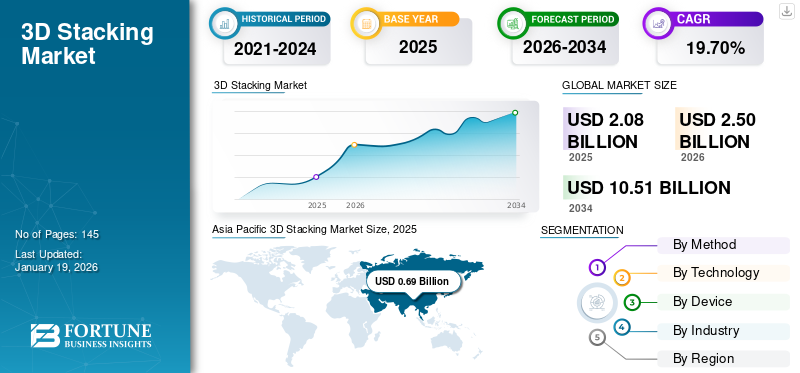
The global 3D stacking market size was valued at USD 2.08 billion in 2025. The market is projected to grow from USD 2.50 billion in 2026 to USD 10.51 billion by 2034, exhibiting a CAGR of 19.70% over the forecast period.
3D stacking, also known as 3D integration or 3D IC stacking, is an advanced semiconductor packaging technology that involves vertically stacking multiple layers of integrated circuits (ICs) or dies into a single compact package. These stacked layers are interconnected using Through-Silicon Vias (TSVs), micro-bumps, or wafer-to-wafer/chip-to-wafer bonding, enabling faster data transfer and improved performance.
Rapid expansion of semiconductor applications across various industries and integration of advanced electronics within the automotive sector indicate major opportunities that lie ahead for the market growth. Moreover, the growing adoption of 3D stack technology to provide shorter interconnects and reduce power consumption further subsidizes the market growth. This technology enables faster data processing and decreases latency, promoting data analytics, machine learning, and cloud computing.
Different companies operating in the market including Taiwan Semiconductor Manufacturing Company Limited (TSMC), Samsung Electronics Co., Ltd., Advanced Micro Devices Inc., Cadence Design Systems, Inc., Texas Instruments Inc., and others. These players have adopted various strategies to strengthen their market positions and increase market penetration in the 3D stacking industry. For instance,
- In September 2024, Samsung announced its plans to mass-produce 3D stacked System-on-Chip (SoC) in 2026. The company aims to enhance performance and address the challenges of semiconductor miniaturization by stacking semiconductors with different functionalities.
The semiconductor industry is sensitive to global supply chain disruptions, as seen during the COVID-19 pandemic. The demand caused by the pandemic had strained capacity at all supply chain points, starting with component suppliers. The COVID-19 pandemic kickstarted the chip shortage, and its long-reaching impacts, including virus outbreaks, labor challenges, and geopolitical uncertainties have fueled it. This had temporarily hampered market growth; however, the industry is expected to reach its pre-pandemic levels over the coming years.
Download Free sample to learn more about this report.
IMPACT OF GENERATIVE AI
Adoption of Generative AI for Accelerating the Design and Simulation Process to Boost the Market Expansion
Generative AI significantly influences the market expansion, particularly within the semiconductor sector. This impact is apparent across several fields, including design innovation, manufacturing efficiency, and market dynamics.
Generative AI improves the design phase of 3D stack by automating the creation of improved layouts and simulations. Tools including generative design algorithms enable engineers to explore various design possibilities, leading to more efficient and innovative 3D stacked architectures. This acceleration in design processes is crucial as the industry seeks to meet the rising needs of applications such as artificial intelligence (AI) and high-performance computing.
MARKET DYNAMICS
3D Stacking Market Trends
Advancements in Chip Packaging Technologies to Drive the Market Growth
The diverse applications of 3D stack technologies propel the 3D stacking market growth. Key platforms such as 3D NAND, 3D SoC, and CBA DRAM, along with technologies including 3D stacked memory, play a crucial role in addressing modern electronics' power, miniaturization, and performance requirements. Chiplet-based designs and heterogeneous integration are reshaping semiconductor architecture. Major industry players including Intel, TSMC, Nvidia, and AMD are investing substantially in these solutions, by utilizing hybrid bonding to enhance interconnect pitches.
In the coming years, trends such as 3.5D packaging and panel-level packaging are expected to significantly influence the market, driven by growing demand from high-performance computing and AI solutions. The competitive landscape is shifting as foundries and IDMs advance their packaging capabilities, while new entrants from China intensify competition. With traditional chip miniaturization nearing its physical limits, the industry is progressively adopting advanced packaging techniques to improve performance and integration.
Market Drivers
Surge in Demand for AI and Data Center Fuels the Market Growth
The demand for data centers has already surged due to the increasing importance of data in today's world. However, this demand is expected to grow further with the rise of generative AI (gen AI). 3D chip stacking technology positively impacts the data centers, unlocking new opportunities for cost optimization.
Data center infrastructure worldwide is rapidly evolving to support AI capabilities, enabling the processing of large volumes of complex computations and requirements. The Asia Pacific and North American regions currently lead in data center proliferation, with key hubs in cities including Beijing, Shanghai, northern Virginia, and the San Francisco Bay Area. According to a 2024 report by the IBM Institute for Business Value (IBM IBV), 43% of C-level technology executives have expressed growing concerns about their technology infrastructure over the past six months due to the rise of generative AI, allowing them to focus on optimizing their infrastructure to put up its scaling needs.
Noteworthy investments from major tech companies also indicates a strong growth for the AI data center sector. In 2025, Microsoft intends to invest around USD 80 billion in data center construction, while Meta dedicates USD 10 billion to a new, four million-square-foot hyperscale data center project in Louisiana.
Market Challenges
Manufacturing Complexities and Increased Cost Hinders 3D Stacking Market Advancement
One of the key challenges in implementing 3D chip stacking is the increased manufacturing complexity. The process demands advanced fabrication techniques and highly specialized equipment, which can significantly raise the production costs. Additionally, this complexity may result in yield issues, further impacting manufacturing competence and effectiveness.
Moreover, the materials essential for 3D stack—such as silicon interposers, through-silicon vias (TSVs), and fine-pitch micro-bumps—contribute to elevated production costs. These components necessitate sophisticated manufacturing processes, driving up material and process expenditures. Guaranteeing compatibility with existing hardware architectures, software interfaces, and thermal management systems often necessitates significant investment and system-level modifications. As a result, these challenges can slow down the broader adoption of 3D stack technologies.
Download Free sample to learn more about this report.
Market Opportunities
Active Government Initiatives and Investments to Cater to New Growth Avenues
Government programs including the U.S. CHIPS and Science Act are facilitating significant investments in semiconductor manufacturing. These initiatives aim to enhance domestic production capabilities and reduce reliance on foreign supply chains, creating opportunities to grow advanced packaging technologies, including 3D stacking. For instance,
- In June 2025, Micron Technology Inc. announced a landmark investment of approximately USD 200 billion in U.S.-based manufacturing and R&D, underscoring America’s efforts to regain leadership in the global semiconductor industry. This expansion is significantly backed by the U.S. government, with Micron expected to receive around USD 6.5 billion in support under the CHIPS and Science Act.
Furthermore, significant investments by industry leaders—such as TSMC’s USD 2.9 billion chip-packaging facility and Fujifilm’s USD 110 million expansion in chip-polishing capabilities—highlight Taiwan’s ongoing commitment to advancing semiconductor excellence.
SEGMENTATION ANALYSIS
By Method
Die-to-Wafer 3D Stacking for Custom Chip Solution Drives the Segmental Growth
Based on method, the market is segmented into die-to-die, die-to-wafer, wafer-to-wafer, chip-to-chip, and chip-to-wafer.
The die-to-wafer method is expected to gain the largest market share, accounting for 28.08% in 2026. owing to its ability to meet the demands for high-performance, cost-effective, and reliable semiconductor packaging. The D2W method allows for integrating different types of dies (e.g., logic, memory, sensors) into a single package. This is significant for evolving applications that need custom chip solutions, such as AI, 5G, and IoT, thus growing the potential market for 3D stack technologies. For instance,
- In May 2025, SUSS, a global semiconductor equipment and process solutions provider, launched the XBC300 Gen2 D2W platform—an advanced bonding solution that improves its hybrid bonding portfolio. This new platform supports die-to-wafer (D2W) bonding on 200mm and 300mm substrates, addressing stringent inter-die spacing requirements and allowing high-precision integration for next-generation semiconductor devices.
However, the wafer-to-wafer method is projected to witness the highest CAGR over the forecast period. Wafer-to-wafer connects exhibit rapid growth through their miniature interconnect points and high-yield manufacturing offerings, which makes them ideal for memory incorporation, neuromorphic processing applications, and image sensor technologies.
By Technology
Increasing Adoption of 3D TSV for Advanced Packaging Solutions Catalyses the Segmental Growth
Based on technology the market is segmented into 3D TSV (Through Silicon Via), 3D hybrid bonding, monolithic 3D integration, and others.
In 2026, 3D TSV (Through-Silicon Via) technology is expected to hold the largest market share, accounting for 33.92%. highlighting its critical role in supporting vertical integration within semiconductor devices. TSVs function as vertical electrical connects, facilitating the creation of innovative 3D packages and integrated circuits by directly linking stacked semiconductor dies. This tactic eliminates the need for conventional edge wiring or wirebonding, which was formerly used in stacked packages on organic substrates. Due to their superior performance and compact integration capabilities, TSVs are gradually preferred in fabricating cutting-edge 3D ICs and interposer-based architectures.
3D hybrid bonding is expected to register the highest CAGR during the forecast period, driven by increasing investments in advanced chip-stacking technologies. This bonding method connects metal-to-metal and dielectric-to-dielectric interfaces, considerably reducing interconnect resistance and improving signal integrity. As a result, it delivers superior power efficiency, performance, and scalability—key requirements for AI accelerators, high-performance computing (HPC) processors, and high-speed memory solutions.
By Device
Increasing Demand for High-Bandwidth Memory (HBM) to Boost the Memory Devices Segment’s Expansion
By device, the market is divided into MEMS/sensors, imaging & optoelectronics, logic ICs, memory devices, LEDs, and others.
Memory devices are expected to be pivotal in driving the 3D stacking market, accounting for a share of 27.37% in 2026. fueled by rising demand for higher performance, increased density, and compact form factors. The surge in data-intensive applications—such as artificial intelligence (AI), cloud computing, and high-performance computing (HPC)—has accelerated the adoption of 3D-stacked memory solutions, including 3D NAND, high-bandwidth memory (HBM), and advanced DRAM. In response to the growing need for fast, low-latency memory, leading players including Samsung, Micron, and SK Hynix are investing considerably in 3D NAND stacking and TSV-based HBM technologies to enhance memory density while enhancing energy effectiveness.
The logic ICs are expected to register the highest CAGR between 2025 and 2032. The growing heterogeneous computing workloads, machine learning (ML) complexity, and artificial intelligence (AI) are driving the demand for 3D stacked logic ICs, specifically for FPGAs, AI accelerators, and processors. For instance,
- In August 2024, Powerchip Semiconductor Manufacturing Company (PSMC) introduced its 2.5D interposers with Logic-DRAM multi-layer wafer stacking technology, to address the growing demands of AI applications. According to the company, major players—including AMD—plan to leverage this technology with advanced logic nodes from leading foundries to develop high-capacity, low-power, high-bandwidth 3D AI chips.
By Industry
To know how our report can help streamline your business, Speak to Analyst
Rising 5G Network Infrastructure and Need for Low-Latency Solutions to Drive 3D Stacking Adoption in IT & Telecom
By industry, the market is segmented into IT & telecom, consumer electronics, automotive, manufacturing, healthcare, and others.
The IT & telecom sector is projected to grow with a highest CAGR during the forecast period, driven by the rapid growth in data consumption, rise of 5G and related technology, and increasing need for high-performance, compact, and energy-efficient semiconductor solutions. The roll-out of 5G networks is one of the primary drivers for growing adoption of 3D stack technology in the telecom sector. As 5G requires higher data speeds, low latency, and more efficient communication between network nodes, 3D stacked semiconductors offer the necessary performance improvements.
- In June 2025, Soitec, a provider of semiconductor materials, announced a strategic partnership with Powerchip Semiconductor Manufacturing Company (PSMC). Under this collaboration, Soitec agrees to supply PSMC with 300mm substrates featuring a release layer and Transistor Layer Transfer (TLT) readiness. This will back the advanced 3D chip stacking at the wafer level, showcasing the potential of next-generation semiconductor technologies.
The consumer electronics industry held the largest market share in 2024, driven by the growing adoption of high-performance tablets, smart wearables, and smartphones integrated with AR/VR capabilities. These devices demand energy-efficient, high-speed processing, and compact consumer-grade 3D stacked memory solutions such as 3D NAND and HBM, together with advanced logic ICs, to enhance battery life and complete device performance.
3D STACKING MARKET REGIONAL OUTLOOK
Geographically, the market is studied into Asia Pacific, North America, South America, Europe and Middle East & Africa.
Asia Pacific
Asia Pacific 3D Stacking Market Size, 2025 (USD Billion)
To get more information on the regional analysis of this market, Download Free sample
Asia Pacific dominated the market with a valuation of USD 0.69 billion in 2025 and is projected to reach USD 0.82 billion in 2026. Asia Pacific held the largest share of the 3D stacking market in 2024, driven by the region's competitive advantages. These include the availability of low-cost labor in China, continuous innovations by fabrication plants in Taiwan, strong manufacturing capabilities of Japanese companies, and the establishment of new semiconductor fabs across China, Taiwan, Japan, and South Korea. The Japan market is projected to reach USD 0.19 billion by 2026, the China market is projected to reach USD 0.23 billion by 2026, and the India market is projected to reach USD 0.11 billion by 2026.
Government support is further fast-tracking the growth of the market in Asia Pacific. Japan’s USD 11.6 billion investment in semiconductor technology development in 2023, with 30% allocated to advanced packaging and 3D stacking, is considerably boosting industry expansion. Similarly, South Korea’s commitment of USD 427 billion in semiconductor investments by 2030 (Ministry of Trade, Industry, and Energy) is strengthening the region's semiconductor ecosystem.
The Chinese market held the largest market share in the Asia Pacific region in 2024. The market's growth is primarily driven by the rapid expansion of domestic semiconductor manufacturing, supported by government initiatives including China’s "Made in China 2025" plan. Additionally, the country's leadership in AI and IoT applications, which rely heavily on heterogeneous integration and high-bandwidth memory (HBM), is fueling the demand. The surge in the need for 5G chipsets, AI processors, and electronics for autonomous vehicles further fastens the adoption of advanced wafer-level 3D integration, subsidizing the market growth.
North America
In 2025, North America generated USD 0.53 billion, contributing 25.30% to global market revenue, and is projected to grow to USD 0.65 billion in 2026. North America is expected to experience fastest growth in the 3D stacking industry, fueled by the region's swift adoption of advanced technologies and a high demand for efficient, compact devices across various sectors. Key players in the market, supported by substantial investments in research and development, are driving the innovation. As advanced packaging gains prominence, Arizona emerges as a critical hub for the vital manufacturing process. Consequently, local governments and private sector companies are collaborating to reinforce Arizona's position as a leader in semiconductor manufacturing. The U.S. market is projected to reach USD 0.47 billion by 2026. For instance,
- In February 2024, Amkor announced the approval of its outsourced semiconductor assembly and test (OSAT) facility in Peoria, Arizona. With a USD 2 billion investment, the facility aims to establish a robust packaging center in Arizona while creating 2,000 new jobs for the local workforce, further bolstering the region's semiconductor manufacturing capabilities.
The U.S. is essential in the 3D stacking market, driven by influential tech companies and strong government support. For example, the CHIPS Act, passed in July 2022, allocated USD 52.7 billion to semiconductor initiatives from FY2022 through FY2027, dedicated on manufacturing and research & development. These funds support advancing 3D stack technologies critical for AI and machine learning applications, further solidifying the U.S. as a leader in semiconductor revolution and next-generation chip design.
South America
The South American market will likely register a modest CAGR during the forecast period. The local government has been executing policies to attract investment in technology and semiconductor manufacturing, enhancing infrastructure, and offering incentives for R&D in the semiconductor sector. Companies including Rohm Semiconductor and Hitachi High Technologies are establishing a presence in Brazil, contributing to developing advanced packaging capabilities, including 3D stacking. Latin America accounted for USD 0.18 billion in 2025, representing 8.80% of the global market share, and is projected to reach USD 0.21 billion in 2026.
Europe
The Europe market accounted for USD 0.42 billion in 2025, representing 20.40% of the global industry, and is expected to reach USD 0.52 billion in 2026. Europe is poised to capture a significant market share during the forecast period, driven by the region's growing digitalization across industries and the growing demand for electronic devices. To meet the expanding need for advanced electronics, companies invest in cutting-edge technologies and expand their production capacities, placing Europe as a key player in the market. The U.K. market is projected to reach USD 0.10 billion by 2026, while the Germany market is projected to reach USD 0.11 billion by 2026.
Germany’s robust automotive industry, driven by the development of electric vehicles (EVs), autonomous driving, and advanced driver assistance systems (ADAS), is fueling the demand for high-performance and energy-efficient semiconductors. These requirements support the growth of 3D stack, which enhances transistor density and accelerates data processing. Additionally, the rapid advancement of Industry 4.0, bolstered by Germany’s leadership in edge computing technology, is driving the increased implementation of 3D-stacked chips in industrial IoT systems.
Middle East & Africa
The Middle East & Africa market generated USD 0.26 billion in 2025, representing 12.40% of the global market landscape, and is expected to reach USD 0.3 billion in 2026. The Middle East & Africa, particularly the UAE and Saudi Arabia, are undergoing moderate CAGR driven by increasing digitalization and government initiatives. As part of its Vision 2030 initiative, Saudi Arabia is making noteworthy investments to establish local semiconductor manufacturing capabilities, addressing the region’s concentrated supply chain. Meanwhile, the UAE’s investment in smart city infrastructure is fueling the demand for advanced semiconductor solutions, including 3D stack technologies, to support IoT devices and high-performance computing systems.
COMPETITIVE LANDSCAPE
Key Industry Players
Market Players Undertake Active R&D Investments and Collaboration Activities to Gain Competitive Edge
Key players in the market actively engage in R&D to innovate and advance 3D stacking technologies, focusing on enhancing performance, reducing costs, and addressing manufacturing challenges. These companies also enter into strategic partnerships with industry leaders and research institutions to leverage expertise and quicken the adoption of 3D stack solutions.
- In February 2024, Samsung accelerated its 3D packaging capabilities by launching a hybrid bonding production line at its advanced packaging hub in Korea. The company has partnered with Applied Materials and Besi Semiconductor to install hybrid bonding equipment at its Cheonan Campus, a critical site for advanced packaging production.
Long List of Companies Studied (including but not limited to)
- Taiwan Semiconductor Manufacturing Company Limited (TSMC) (Taiwan)
- Intel Corporation (U.S.)
- Samsung Electronics Co., Ltd. (South Korea)
- Advanced Micro Devices Inc. (U.S.)
- Advanced Semiconductor Engineering Inc. (Taiwan)
- Texas Instruments Inc. (U.S.)
- Amkor Technology Inc. (U.S.)
- Tektronix Inc. (U.S.)
- Broadcom Inc. (U.S.)
- Cadence Design Systems, Inc. (U.S.)
- IBM Corporation (U.S.)
- Marvell Technology, Inc. (U.S.)
- Lightmatter (U.S.)
- Kioxia Corporation (Japan)
- JCET Group (China)
- Graphcore (U.K.)
….and more
KEY INDUSTRY DEVELOPMENTS
- June 2025: Cadence Design Systems, Inc. has expanded its collaboration with Samsung Foundry through a multi-year IP agreement, extending Cadence’s memory and interface IP solutions across Samsung Foundry’s SF5A, SF2P, and SF4X advanced process nodes. This partnership enhances multi-die planning and implementation by offering reference flows and package design kits, built on the Cadence Integrity 3D-IC platform, which integrates packaging, system-level analysis, and system planning.
- June 2025: Soitec, a France-based semiconductor materials company, has announced a collaboration with Powerchip Semiconductor Manufacturing Corporation (PSMC). As part of the agreement, Soitec will supply PSMC with 300mm substrates featuring a release layer and Transistor Layer Transfer (TLT) readiness, supporting a new demonstration of advanced 3D chip stacking at the wafer level.
- April 2025: Intel has unveiled its next-generation 14A (1.4nm) node as part of its updated hardware roadmap. The company also introduced its 18A-P and 18A-PT nodes. The 18A-P node is a high-performance variant of the 18A, while the 18A-PT supports Through Silicon Vias (TSVs) for 3D chip stacking. Intel’s T-series nodes also integrate Foveros Direct 3D technology, which shares characteristics similar to those of TSMC’s 3D chip stacking technology.
- January 2025: Samsung Foundry had partnered with Dreambig Semiconductor to develop the MARS chip label platform, introducing the Networking IO and Chiplet Hub chiplets. This collaboration leverages Samsung Foundry’s advanced 3D chip-on-wafer stacking and SF4X FinFET process technology. With its extensive expertise in HBM memory and synergistic advanced packaging, Samsung Foundry works closely with Dreambig Semiconductor to advance the platform’s capabilities.
- November 2024: Lightmatter, a photonic supercomputing company, announced a strategic collaboration with Advanced Semiconductor Engineering, Inc. This partnership aims to advance Lightmatter’s Passage platform, a 3D-stacked photonics engine with pluggable fiber, to address the critical AI interconnect bottlenecks currently limiting data center infrastructure performance.
- August 2024: TSMC introduced its 3DFabric family of technologies, including 2D and 3D frontend and backend interconnect solutions. The TSMC-SoIC (System on Integrated Chips) frontend technologies implement the precision and methodologies of edge silicon fabs, essential for 3D silicon stacking. The die stacking process incorporates Wafer-on-Wafer (WoW) and Chip-on-Wafer (CoW) technologies, enabling the 3D stacking of identical and heterogeneous dies.
INVESTMENT ANALYSIS AND OPPORTUNITIES
The 3D stacking industry is poised for substantial growth, driven by technological advancements, strategic investments, and supportive government policies. By focusing on advanced packaging solutions, R&D initiatives, and strategic partnerships, stakeholders can capitalize on the emerging opportunities in this dynamic sector. For instance,
- In June 2025, GlobalFoundries, together with the Trump Administration and leading technology companies such as SpaceX, Apple, Qualcomm Technologies, Inc., AMD, GM, and NXP, aiming to onshore critical components of their supply chain, announced plans to invest USD 16 billion to develop its advanced packaging and semiconductor manufacturing capabilities across its facilities in Vermont and New York.
REPORT COVERAGE
The report provides a detailed analysis of the market and focuses on key aspects such as leading companies, product/service types, and leading applications of the product. Besides, the report offers insights into the market trends and highlights key industry developments. In addition to the factors above, the report encompasses several factors that contributed to the growth of the market in recent years.
Request for Customization to gain extensive market insights.
REPORT SCOPE & SEGMENTATION
|
ATTRIBUTE |
DETAILS |
|
Study Period |
2021-2034 |
|
Base Year |
2025 |
|
Estimated Year |
2026 |
|
Forecast Period |
2026-2034 |
|
Historical Period |
2021-2024 |
|
Growth Rate |
CAGR of 19.70% from 2026 to 2034 |
|
Unit |
Value (USD Billion) |
|
Segmentation |
By Method
By Technology
By Device
By Industry
By Region
|
|
Companies Profiled in the Report |
Taiwan Semiconductor Manufacturing Company Limited (TSMC) (Taiwan), Intel Corporation (U.S.), Samsung Electronics Co., Ltd. (South Korea), Advanced Micro Devices Inc. (U.S.), Advanced Semiconductor Engineering Inc. (Taiwan), Texas Instruments Inc. (U.S.), Amkor Technology Inc. (U.S.), Tektronix Inc. (U.S.), Broadcom Inc. (U.S.), Cadence Design Systems, Inc. (U.S.), etc. |
Frequently Asked Questions
The market is projected to reach USD 10.51 billion by 2034.
In 2025, the market was valued at USD 2.08 billion.
The market is projected to grow at a CAGR of 19.70% during the forecast period.
In terms of market share, the 3D TSV segment leads the market.
Surge in AI and data center demands fuels the market growth.
Taiwan Semiconductor Manufacturing Company Limited (TSMC), Intel Corporation, Samsung Electronics Co., Ltd., Advanced Micro Devices Inc., Advanced Semiconductor Engineering Inc., Cadence Design Systems, Inc., Texas Instruments Inc., are the top players in the market.
North America is expected to hold the highest market share.
By industry, the IT & telecom sector is expected to grow with a highest CAGR during the forecast period.


- 2021-2034
- 2025
- 2021-2024
- 145
Get 30-60 hrs Free Customization
Expand Regional and Country Coverage, Segments Analysis, Company Profiles, Competitive Benchmarking, and End-user Insights.
Related Reports
-
US +1 833 909 2966 ( Toll Free )
-
Get In Touch With Us