Cloud EDA Market Size, Share & Industry Analysis, By Deployment (Public Cloud, Private Cloud, and Hybrid Cloud), By Enterprise Type (Large Enterprises and Small & Medium-sized Enterprises (SMEs)), By Application (Digital IC Design, Analog & Mixed-Signal IC Design, Advanced SoC Design, and PCB & System-Level Design), By Industry (Consumer Electronics, Automotive, Aerospace & Defense, Healthcare, Telecommunication, and Others), and Regional Forecast, 2026 – 2034

(Offer valid till 30th Jun 2026)
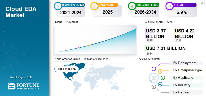
CLOUD EDA MARKET SIZE AND FUTURE OUTLOOK
The cloud EDA market size was valued at USD 4.13 billion in 2025. The market is projected to grow from USD 4.41 billion in 2026 to USD 7.67 billion by 2034, exhibiting a CAGR of 7.2% during the forecast period. North America dominated the cloud eda market with a market share of 41.64% in 2025.
Cloud Electronic Design Automation (EDA) solutions are advanced digital platforms that enable semiconductor companies and electronics manufacturers to design, simulate, verify, and optimize integrated circuits and electronic systems using scalable cloud infrastructure. Unlike traditional on-premise EDA environments, cloud-based platforms provide elastic computing power, collaborative design access, and flexible deployment models that support increasingly complex chip architectures, including advanced node, system-on-chip, and heterogeneous integration designs.
The rapid evolution of technologies such as artificial intelligence, 5G connectivity, high-performance computing, and IoT devices is significantly increasing chip design complexity and computational requirements. As semiconductor development cycles shrink and competition intensifies, organizations are turning to cloud EDA solutions to accelerate verification workloads, enable parallel simulations, and reduce infrastructure constraints. Cloud deployment also supports geographically distributed engineering teams, improving collaboration and shortening time-to-market.
Key players such as Synopsys Inc., Cadence Design Systems, Inc., Keysight Technologies and Altium Limited are expanding their cloud-enabled portfolios through platform integration, AI-driven design automation, and strategic collaborations with semiconductor manufacturers and hyperscale cloud providers. Their focus remains on delivering secure, high-performance, and scalable design environments that meet the growing computational and verification demands of next-generation semiconductor innovation.
Download Free sample to learn more about this report.
IMPACT OF GENERATIVE AI
Generative AI Transforms Cloud EDA Workflows and Strengthen Market Growth
Generative AI is increasingly shaping the cloud EDA market by improving chip design productivity, automating complex workflows, and reducing design cycle times. Semiconductor companies are adopting AI-driven EDA tools for design space exploration, verification, layout optimization, and bug detection. Since these AI models require high computing power and large datasets, cloud-based EDA platforms are becoming important for supporting scalable and faster design environments. For instance,
- In March 2026, Siemens launched its Fuse EDA AI Agent to integrate generative AI into chip design workflows, enabling automated task execution, improved engineering productivity, and faster semiconductor development cycles.
AI-assisted EDA tools help engineers evaluate multiple design options, optimize power-performance trade-offs, and reduce manual effort. Cloud infrastructure supports these capabilities through parallel processing, large-scale simulations, and centralized data access. For instance,
- In April 2025, Cadence highlighted the role of AI-driven design tools in accelerating verification cycles and improving design efficiency across advanced semiconductor nodes.
CLOUD EDA MARKET TRENDS
Rising Demand for Cloud-based Verification and Emulation Services to Strengthen Market Expansion
The market is witnessing a growing shift toward cloud-based verification and emulation services as semiconductor companies face increasing SoC complexity, larger software stacks, and tighter development timelines. Verification activities such as regression testing, power analysis, and system validation require high compute capacity, making scalable cloud infrastructure more efficient than traditional on-premise setups. This is particularly important for AI, automotive, networking, and data center chips, where validation demands are rapidly increasing.
The trend is further supported by the need to validate complex AI and billion-gate designs earlier in the design cycle. Cloud-based verification and emulation enable flexible access to large-scale compute resources, especially during peak workloads and critical milestones, reducing reliance on internal hardware expansion. For instance,
- In August 2025, Cadence and NVIDIA introduced hardware-accelerated dynamic power analysis using the Palladium Z3 Enterprise Emulation Platform, enabling billion-gate design analysis within hours with up to 97% accuracy.
These developments indicate that cloud-based verification and emulation are becoming a strategic component of semiconductor development, driving greater adoption of cloud EDA solutions.
MARKET DYNAMICS
MARKET DRIVERS
Download Free sample to learn more about this report.
Growing Demand for Faster Chip Design Cycles to Fuel Market Growth
The growing need to accelerate chip design cycles is a key driver of the cloud EDA market growth. Semiconductor companies are under constant pressure to shorten development timelines, enhance verification processes, and achieve faster tape-out, particularly for advanced applications such as artificial intelligence, high-performance computing, automotive systems, and complex system-on-chip designs.
Cloud-based EDA platforms enable design teams to access scalable computing resources on demand, execute parallel workloads efficiently, and minimize bottlenecks across simulation, timing sign-off, and physical verification. This capability significantly improves overall design efficiency and supports faster commercialization of semiconductor products. Industry developments further highlight this trend. For instance,
- In October 2025, Synopsys stated that chip design workloads can run up to 52x faster on Synopsys Cloud SaaS, leveraging advanced cloud compute resources and on-demand FlexEDA licensing, enabling accelerated tape-out and faster timing signoff.
- In June 2025, Siemens stated at DAC 2025 that its AI-enhanced EDA toolset is designed to improve productivity, accelerate innovation, and speed time-to-market for semiconductor and PCB design flows.
- In March 2025, Synopsys collaborated with NVIDIA, which is projected to accelerate circuit simulation by up to 30x on the NVIDIA GB200 Grace Blackwell platform, highlighting how high-performance cloud and accelerated computing are being used to compress EDA runtimes.
Similarly, growing pressure to achieve first-pass silicon success is prompting companies to conduct deeper, more comprehensive verification and validation cycles within limited timelines. This is increasing dependence on cloud-based EDA environments that can handle intensive workloads more efficiently.
MARKET RESTRAINTS
Data Security and Intellectual Property Concerns Restraint Market Growth
Data security and intellectual property protection concerns remain a major restraint for the market. Semiconductor design data, including chip architecture, layouts, and verification files, represents high-value intellectual property and significant R&D investments. This makes companies cautious about shifting design workloads to cloud environments due to risks such as data breaches, unauthorized access, and cyber threats. Ensuring secure access, encryption, and controlled environments continues to be a key challenge for wider adoption. For instance,
- In March 2025, Synopsys highlighted that security and IP protection remain among the top concerns for semiconductor firms when adopting cloud-based EDA workflows, particularly for advanced-node and defense-related designs.
- In October 2024, the U.S. National Institute of Standards and Technology (NIST) emphasized that semiconductor design data requires stringent cybersecurity frameworks due to its high sensitivity and strategic importance.
In addition, strict internal policies and regulatory requirements often push companies to retain control over their design environments, limiting the use of shared cloud infrastructure and increasing preference for private or hybrid cloud models. Concerns related to data residency, encryption standards, and secure collaboration across distributed teams further slower product adoption.
MARKET OPPORTUNITIES
Rising Expansion of Edge Devices and IoT Chip Design to Create Market Growth Opportunities
The rapid growth of edge computing and IoT devices is creating strong opportunities for the market. Sectors such as smart homes, industrial automation, healthcare, automotive, and telecommunications are increasingly using connected devices that require low-power and application-specific chips. Designing these chips involves balancing performance, power efficiency, size, and cost, which increases the need for advanced simulation, verification, and optimization tools. Cloud EDA platforms support these requirements by offering scalable computing resources, faster design iterations, and flexible design environments without the need for heavy infrastructure investment. For instance,
- In January 2025, Ericsson projected that global IoT connections would exceed 29 billion by 2027, driven by growth in massive IoT and broadband IoT applications, highlighting the rising demand for connected devices and associated semiconductor design.
These developments indicate that the expansion of edge devices and IoT ecosystems is widening semiconductor design opportunities and creating strong growth potential for cloud EDA platforms.
Segmentation Analysis
By Industry
Consumer Electronics Dominates Due to High Device Volume and Rapid Innovation
Based on the industry, the market is classified into consumer electronics, automotive, aerospace and defense, healthcare, telecommunication, and others.
Consumer electronics held majority share of the market in 2024. In 2025, the segment dominated with a 34.5% of share, as it produces a large volume of devices, including smartphones, laptops, wearables, and smart home gadgets, all of which require highly complex integrated circuits and system-on-chip designs. Rapid innovation cycles, intense competition, and the push for smaller, more efficient, and feature-rich devices increase design complexity, making scalable cloud-based EDA tools essential for faster, cost-effective development and real time collaboration across a global R&D team.
Automotive is expected to witness the highest CAGR of 9.2% during the forecast period.
To know how our report can help streamline your business, Speak to Analyst
By Deployment
Hybrid Cloud Deployment Leads Market Fueled by Scalability and IP Security Needs
Based on the deployment, the market is divided into public cloud, private cloud, and hybrid cloud.
Hybrid cloud held the majority share by deployment in 2024. In 2025, the segment held a share of 51.4% as it combines the benefits of both on premise and cloud environments. Companies can continue using their existing infrastructure for sensitive or legacy workloads while leveraging the cloud for high-performance computing, scalability, and large-scale simulation. This approach ensures cost efficiency, flexibility, and better control over intellectual property, which is crucial in semiconductor design.
Public cloud is expected to witness the highest CAGR of 10.3% during the forecast period.
By Enterprise Type
Large Enterprises Hold Majority Share Due to Complex Designs and High Compute Requirements
Based on enterprise type, the market is categorized into large enterprises and Small & Medium-sized Enterprises (SMEs).
Large enterprises held majority share of the market in 2024. It has the resources, complex design requirements, and high-volume chip development needs that justify investment in cloud-based EDA solutions. These organizations often work on advanced semiconductor designs, such as system-on-chip (SoC) and AI/5G-enabled devices, which require massive compute power and high-performance simulation that cloud platforms provide.
Small & Medium-sized Enterprises (SMEs) are expected to witness the highest CAGR of 10.3% during the forecast period.
By Application
Digital IC Design Leads Owing to Complexity and Continuous Demand in Electronics
Based on the application, the market is segmented into digital IC design, analog & mixed-signal IC design, advanced SoC design, and PCB & system-level design.
Digital IC design held the majority share in 2024. In 2025, the segment was at a share of 43.8% as most modern electronic devices rely heavily on digital circuits such as microprocessors, memory chips, and system-on-chip components. Digital designs are highly complex and computationally intensive, requiring extensive simulation, verification, and optimization, which benefit greatly from the scalability and high-performance computer power of cloud-based EDA tools.
Advanced SoC design is expected to witness the highest CAGR of 10.1% during the forecast period.
Cloud EDA Market Regional Outlook
By region, the market is categorized into North America, South America, Europe, Middle East & Africa, and Asia Pacific.
North America
North America Cloud EDA Market Size, 2025 (USD Billion)
To get more information on the regional analysis of this market, Download Free sample
North America holds the majority cloud EDA market share due to its deep-rooted semiconductor innovation ecosystem, high R&D intensity, and strong demand for advanced chip design across strategic industries. The U.S., in particular, leads in the development of AI accelerators, data center processors, aerospace electronics, and defense-grade semiconductors, all of which require compute-intensive verification and large-scale simulation workloads that are well suited to cloud environments.
Federal initiatives such as the CHIPS and Science Act are accelerating domestic semiconductor design and advanced node research, further increasing reliance on scalable cloud-based EDA platforms. Additionally, the region’s robust venture capital landscape and startup ecosystem in silicon design, especially in AI and custom silicon, drive early adoption of flexible cloud licensing models. The combination of high-value chip programs, strong digital infrastructure, and sustained investment in next-generation computing technologies positions North America as the leading regional market.
North America market held the largest market at USD 1.72 billion in 2025.
U.S. Cloud EDA Market
Given North America’s strong contribution, the U.S. market was at USD 1.54 billion in 2025, accounting for roughly 37.2% of sales.
Europe
Europe is projected to grow at 5.6% over the coming years and reached a valuation of USD 0.51 billion in 2025, driven by accelerating efforts to achieve semiconductor self-sufficiency, automotive chip innovation, and advanced industrial electronics development. The region’s strong presence in automotive semiconductor design, particularly in Germany and France, is driving demand for high-reliability, power-efficient chip architectures that require advanced simulation and verification capabilities suited to cloud-based EDA environments. Policy initiatives such as the European Chips Act are encouraging domestic semiconductor R&D, funding design innovation, and strengthening local fabrication and design ecosystems.
U.K. Cloud EDA Market
The U.K. market in 2025 was valued at around USD 0.10 billion, representing roughly 2.4% of global revenues.
Germany Cloud EDA Market
Germany’s market reached USD 0.10 billion in 2025, equivalent to around 2.4% of global sales.
Asia Pacific
Asia Pacific is expected to grow at the highest CAGR and reached USD 1.40 billion by 2025, driven by the region’s fast-evolving semiconductor design landscape and its role as the global center of electronics manufacturing. The concentration of consumer electronics production in China, South Korea, Taiwan, and Southeast Asia creates continuous demand for rapid chip customization, reference design modifications, and application-specific integrated circuits, all of which require scalable simulation capacity. The strong foundry ecosystem, particularly the manufacturing dominance of TSMC and Samsung Electronics, encourages closer collaboration between design houses and fabrication facilities, thereby increasing the need for cloud-based verification and tape-out-readiness tools.
Japan Cloud EDA Market
The Japan market in 2025 was valued at around USD 0.15 billion, accounting for roughly 3.6% of global revenues.
China Cloud EDA Market
China’s market is projected to be one of the largest worldwide and 2025 revenues reached at USD 0.43 billion, representing 10.4% of global sales.
India Cloud EDA Market
The India market in 2025 was at USD 0.14 billion, accounting for roughly 3.4% of global market share.
South America and Middle East & Africa
The Middle East & Africa region is expected to grow at the second-highest CAGR in the market. It is due to its accelerating diversification into advanced technology sectors and strategic investments in semiconductor design capabilities. Countries such as the United Arab Emirates and Saudi Arabia are expanding their focus beyond oil-dependent economies toward AI, smart infrastructure, defense electronics, and high-performance computing, which require localized chip design and system development expertise. National digital transformation programs, including Saudi Arabia’s Vision 2030, are fostering technology parks, research centers, and partnerships to build semiconductor and advanced electronics capabilities.
South America is expected to grow at a stable CAGR, driven by gradual increases in electronics manufacturing, automotive semiconductor adoption, and emerging tech startups in countries such as Brazil and Argentina. The region’s moderate but steady investment in cloud infrastructure and growing interest in cost-efficient, scalable design solutions support consistent adoption of cloud-based EDA platforms.
GCC Cloud EDA Market
The GCC market reached USD 0.08 billion in 2025, representing roughly 1.9% of global revenues.
COMPETITIVE LANDSCAPE
Key Industry Players
Leading Cloud EDA Vendors Expand Capabilities Through Strategic Partnerships and Innovation
Key market players in the market space are enhancing their platforms to address the rising demand for scalable, AI-enabled, and collaborative chip design solutions. Companies are pursuing strategic initiatives such as technology partnerships, mergers and acquisitions, and joint development programs to strengthen their cloud offerings, integrate advanced simulation and verification tools, and broaden their global reach. These efforts aim to provide high-performance, secure, and flexible design environments that cater to the increasing complexity of semiconductor and electronics design workflows.
LIST OF KEY CLOUD EDA COMPANIES PROFILED
- Synopsys, Inc. (U.S.)
- Cadence Design Systems, Inc. (U.S.)
- Siemens AG (Germany)
- Keysight Technologies (U.S.)
- Renesas Electronics Corporation (Altium Limited) (Japan)
- Zuken Inc (Japan)
- Silvaco Group, Inc. (U.S.)
- Autodesk, Inc. (U.S.)
- Xpeedic Technology, Inc. (China)
- Empyrean Technology Co., Ltd. (China)
KEY INDUSTRY DEVELOPMENTS
- March 2026: Silvaco Group has expanded its strategic partnership with Advanced Power Electronics Corp. (APEC), with APEC adopting more of Silvaco’s TCAD and EDA tools. This will help accelerate the development of advanced silicon carbide (SiC) power devices while improving performance and time-to-market. The collaboration supports innovation across industries like automotive and renewable energy. It also strengthens both companies’ positions in the growing power electronics market.
- October 2025: Altair released Altair HPCWorks 2026, enhancing its HPC and cloud platform to support cloud-based EDA workloads. The update improves GPU integration, AI-driven resource optimization, Kubernetes connectivity, and advanced reporting, enabling semiconductor and electronic design teams to run large-scale EDA jobs more efficiently in cloud environments.
- April 2025: Altair expanded its footprint in cloud EDA by enhancing its cloud native verification and simulation capabilities for semiconductor and electronic system design. With tools such as DSim, which integrate with major cloud providers and support scalable ASIC and FPGA simulation, Altair is enabling cost-effective, on-demand compute for large-scale regression testing and design verification.
- December 2024: Marvell Technology Inc. partnered with Amazon Web Services in a five-year deal to adopt EDA-in-the-cloud for chip development. The collaboration allows Marvell to leverage AWS cloud EDA solutions to accelerate, scale, and secure semiconductor design across AI products, DSPs, data center interconnect modules, and Ethernet switching silicon.
- March 2024: HCLTech partnered with NetApp and launched a cloud-enabled EDA solution to accelerate semiconductor design workflows. The platform leverages hybrid cloud infrastructure to improve scalability, manage large data volumes, optimize IT resources, and reduce time-to-market for EDA projects while enhancing design quality and reliability.
- March 2024: Synopsys unveiled AI-driven EDA solutions (DSO.ai, VSO.ai, 3DSO.ai) that speed chip design, verification, and multi-die optimization. They also launched Synopsys Cloud Hybrid, which seamlessly bursts on-prem EDA workloads to the cloud. New hardware-assisted verification systems and expanded IP (via Intrinsic ID acquisition) enhance productivity and security in semiconductor design.
REPORT COVERAGE
The report provides a detailed analysis of the market and focuses on key aspects, including leading companies, product types, and the leading applications of the product. Besides, it offers insights into the market trends and highlights key industry developments. In addition to the factors above, the market's growth in recent years was driven by several other factors.
Request for Customization to gain extensive market insights.
Report Scope & Segmentation
| ATTRIBUTE | DETAILS |
| Study Period | 2021-2034 |
| Base Year | 2025 |
| Estimated Year | 2026 |
| Forecast Period | 2026-2034 |
| Historical Period | 2021-2024 |
| Growth Rate | CAGR of 7.2% from 2026-2034 |
| Unit | Value (USD Billion) |
| Segmentation | By Deployment, Enterprise Type, Application, Industry, and Region |
| By Deployment |
|
| By Enterprise Type |
|
| By Application |
|
| By Industry |
|
| By Region |
|
Frequently Asked Questions
According to Fortune Business Insights, the global market value stood at USD 4.13 billion in 2025 and is projected to reach USD 7.67 billion by 2034.
In 2025, the North America market value stood at USD 1.72 billion.
The market is expected to grow at a CAGR of 7.2% over the forecast period.
By industry, the consumer electronic segment is expected to lead the market.
Growing demand for faster chip design cycles to fuel market growth drives market growth.
Synopsys Inc., Cadence Design Systems, Inc., Keysight Technologies and Altium Limited are the major players in the global market.
North America dominated the market in 2025.


- 2021-2034
- 2025
- 2021-2024
- 150
-
(Offer valid till 30th Jun 2026)
Get 30-60 hrs Free Customization
Expand Regional and Country Coverage, Segments Analysis, Company Profiles, Competitive Benchmarking, and End-user Insights.
Related Reports
-
US +1 833 909 2966 ( Toll Free )
-
Get In Touch With Us